Motion estimating method and motion estimating circuit using the method
A motion estimation and circuit technology, applied in TV, electrical components, digital video signal modification, etc., can solve problems such as limited application range, difficulty in VLSI implementation, high hardware cost, etc.
- Summary
- Abstract
- Description
- Claims
- Application Information
AI Technical Summary
Problems solved by technology
Method used
Image
Examples
specific Embodiment approach 1
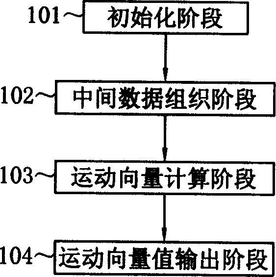
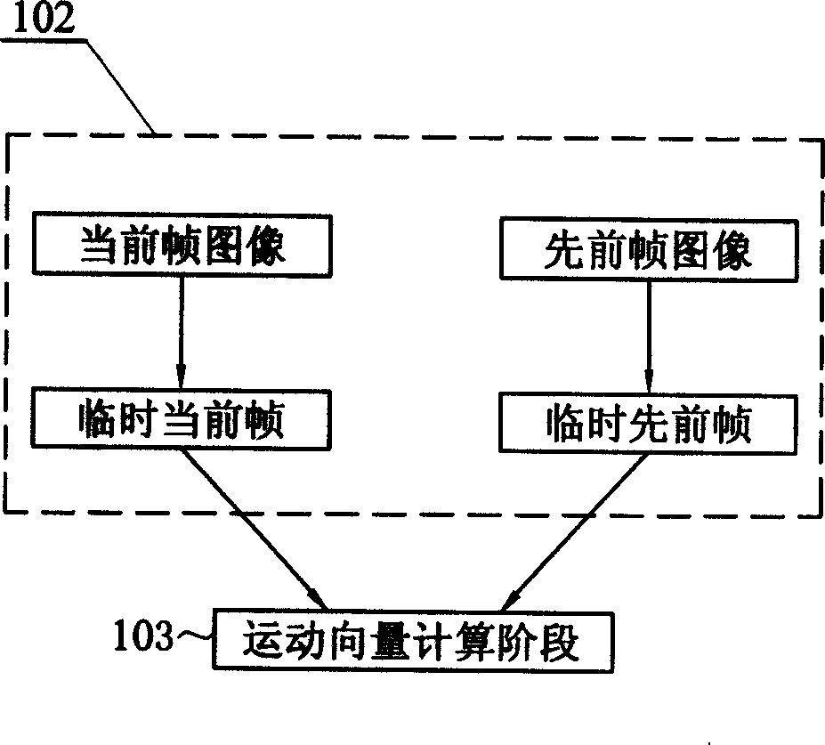
[0070] Specific implementation mode one: the following combination Figure 1 to Figure 3 This embodiment will be specifically described. A method of motion estimation, which is accomplished through the following steps:
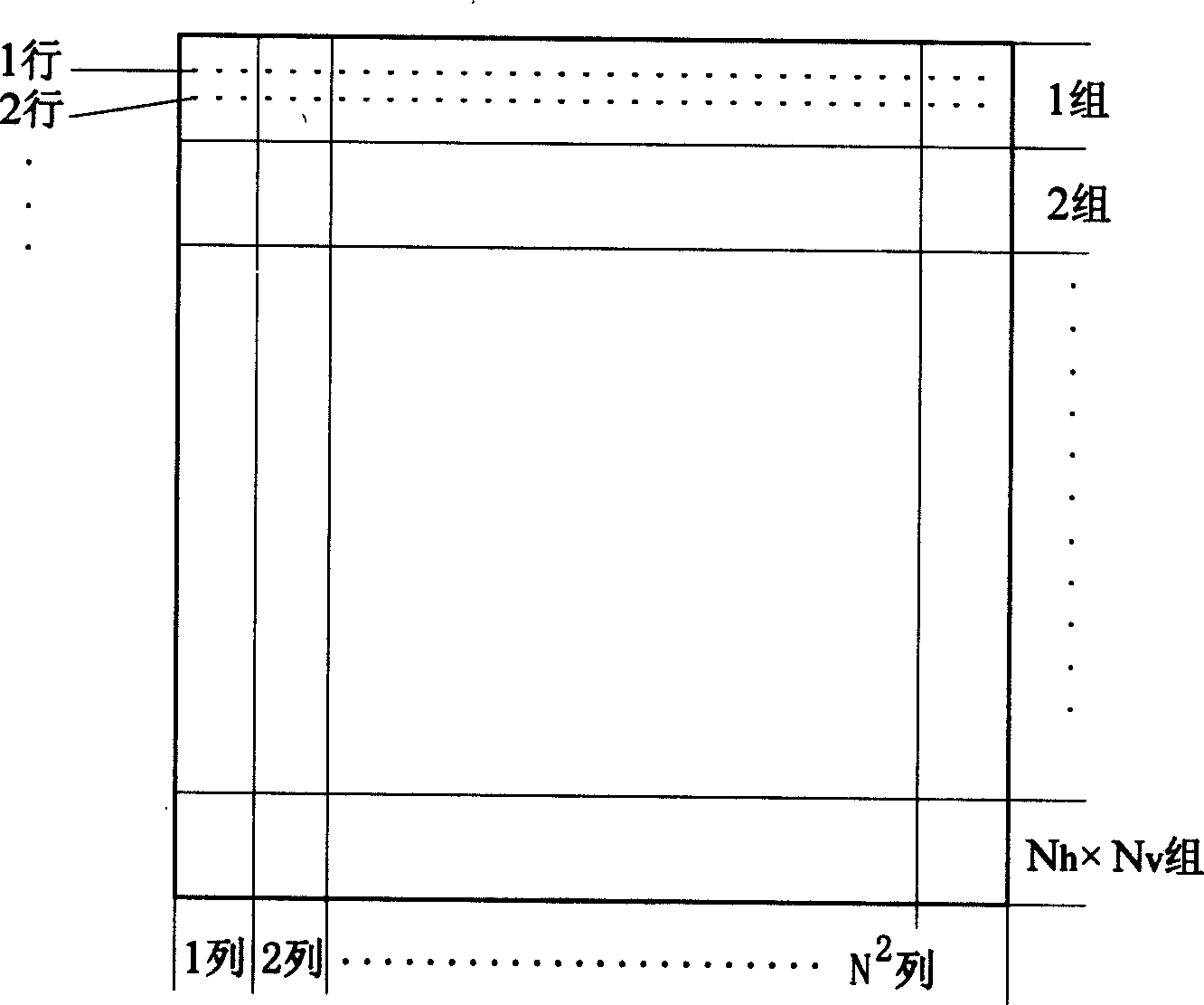
[0071] (1) Initialization stage 101: Initialize two temporary current frame and temporary previous frame images without any pixel data. Each row of these two frames of images contains N 2 pixels, each column contains N h N v (2p+1) 2 pixels; divide the two temporal frames into N in the column direction h N v pixel groups, each group contains (2p+1) 2 columns, each group contains a total of N 2 (2p+1) 2 pixels, named in the order of the columns as Group 1, Group 2...Nth h Nv Group. Take the upper left corner of the frame as the vertex, and use (l, k) to represent the position of the pixel in the previous or current frame image, where 1≤l≤N 2 , 1≤l≤N h N v (2p+1) 2 ;For the current frame image and the previous frame image as input, each row contai...
specific Embodiment approach 2
[0076] Specific implementation mode two: the following combination Figure 5 This embodiment will be specifically described with FIG. 6 . A motion estimation circuit applying a motion estimation method, which consists of N 2 block matching unit (PE 1 -PE N 2 ), bus Y1, bus Y2, bus C1, bus C2, N multiplexers (M 1 -M N ), two first-in-first-out modules (FIFO1, FIFO2), N-2 multiplexers ME 2 -ME N-1 ), N-1 delay registers (Delay 2 -Delay N ), N-1 delay register banks (Delay -1 -Delay -N-1 ), N-1 adders (a 2 -a N ) and the motion vector generation unit MV. Block Matching Unit (PE 1 -PE N 2 ) are arranged into an array structure of N rows and N columns, and the bus Y1 is connected to the multiplexer (M 1 -M N ), an input of the multiplexer (M 1 -M N ) The other input terminals are connected to the bus Y2, the multiplexer M 1 The output terminals of are respectively connected to the block matching unit PE 1 The pin Y_in1 and the input terminal of the first-in-fi...
PUM
 Abstract
Description
Claims
Application Information


