

Mfg method of fall carrier capture structure organic LED
A light-emitting diode, organic technology, applied in semiconductor/solid-state device manufacturing, electrical components, electrical solid-state devices, etc., can solve problems such as poor luminous efficiency, and achieve the effects of high brightness, good spectral color purity, and high efficiency
- Summary
- Abstract
- Description
- Claims
- Application Information
AI Technical Summary
Problems solved by technology
Method used
Image

Examples
Embodiment 1
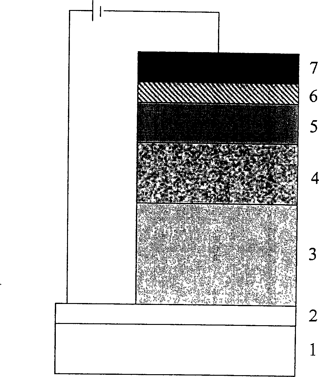
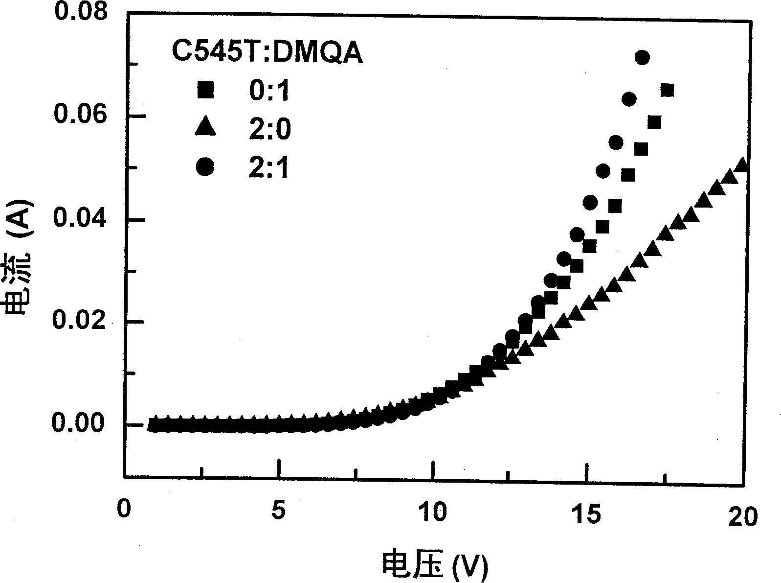
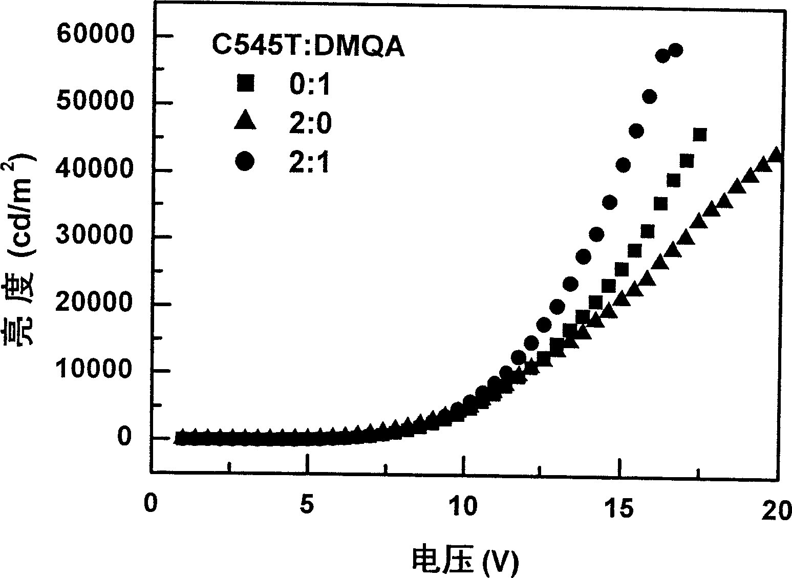
[0025] In a vacuum of 1-5 x 10 -4 In Papa's coating equipment, the hole transport layer NPB, the dye C545T and DMQA double-doped light emitting layer, the electron transport layer Alq 3 , buffer layer LiF and metal Al are vapor-deposited on the ITO of the glass substrate, and the structure is prepared as ITO / NPB / Alq 3 :C545T:DMQA / Alq 3 / LiF / Al organic light-emitting diodes. Light-emitting layer Alq 3 : The weight ratio of C545T: DMQA is controlled at 1: 2%: 1%, the thickness of NPB is 50nm, the doped light-emitting layer is 30nm, and the electron transport layer Alq 3 20nm for LiF, 1nm for LiF, and 200nm for Al. The obtained device is driven by a DC voltage, and the DMQA luminescence with a main peak at 535nm and a half-peak width of 30nm is obtained, the maximum current efficiency is 16.0cd / A, the maximum power efficiency is 11.0lm / W, and the maximum brightness is 60000cd / m 2 . The efficiency and brightness of double-doped devices are higher than those of single-doped 1...
Embodiment 2
[0027] In a vacuum of 1-5 x 10 -4 In Papa’s coating equipment, the hole transport layer NPB, the dyes DCJTI and DCJTB double-doped light-emitting layer, the electron transport layer Alq 3 , buffer layer LiF and metal Al are vapor-deposited on the ITO of the glass substrate, and the structure is prepared as ITO / NPB / Alq 3 :DCJTI:DCJTB / Alq 3 / LiF / Al organic light-emitting diodes. Light-emitting layer Alq 3 : The weight ratio of DCJTI:DCJTB is controlled at 1:1%:1%, the thickness of NPB is 50nm, the doped light-emitting layer is 30nm, Alq 3 20nm for LiF, 1nm for LiF, and 200nm for Al. The obtained device is driven by a DC voltage to obtain red light with a main peak at 625nm and a half-peak width of 74nm, a maximum current efficiency of 5.0cd / A, and a maximum brightness of 10,000cd / m 2 . The efficiency and brightness of double-doped devices are higher than those of single-doped 1% DCJTB, and the color purity of red light is better than that of single-doped.
Embodiment 3
[0029] In a vacuum of 1-5 x 10 -4 In Papa's coating equipment, the hole transport layer NPB, the dye C545T and DCJTI double-doped light emitting layer, the electron transport layer Alq 3 , buffer layer LiF and metal Al are vapor-deposited on the ITO of the glass substrate, and the structure is prepared as ITO / NPB / Alq 3 :C545T:DCJTI / Alq 3 / LiF / Al organic light-emitting diodes. Light-emitting layer Alq 3 : The weight ratio of C545T: DCJTI is controlled at 1: 0.5%: 2%, the thickness of NPB is 50nm, the doped light-emitting layer is 30nm, Alq 3 20nm for LiF, 1nm for LiF, and 200nm for Al. The obtained device is driven by DC voltage, and the red light emission of DCJTI can be obtained, the maximum power efficiency is 9.4lm / W, the maximum current efficiency is 11.2cd / A, and the maximum brightness is 29500cd / m 2 , the main peak of luminescence is 615nm. The efficiency and brightness of double-doped devices are higher than those of single-doped 2% DCJTI, and the color purity of ...
PUM
 Abstract
Description
Claims
Application Information