Drive circuit of picture element array for display panel

A display panel and drive circuit technology, applied to static indicators, TVs, instruments, etc., can solve problems such as shift signal overlap

Active Publication Date: 2005-04-27
AU OPTRONICS CORP
View PDF1 Cites 1 Cited by
  • Summary
  • Abstract
  • Description
  • Claims
  • Application Information

AI Technical Summary

Problems solved by technology

[0005] In view of this, the object of the present invention is to provide a driving circ...

Method used


Image

  • Drive circuit of picture element array for display panel
  • Drive circuit of picture element array for display panel
  • Drive circuit of picture element array for display panel

Examples


Embodiment 1

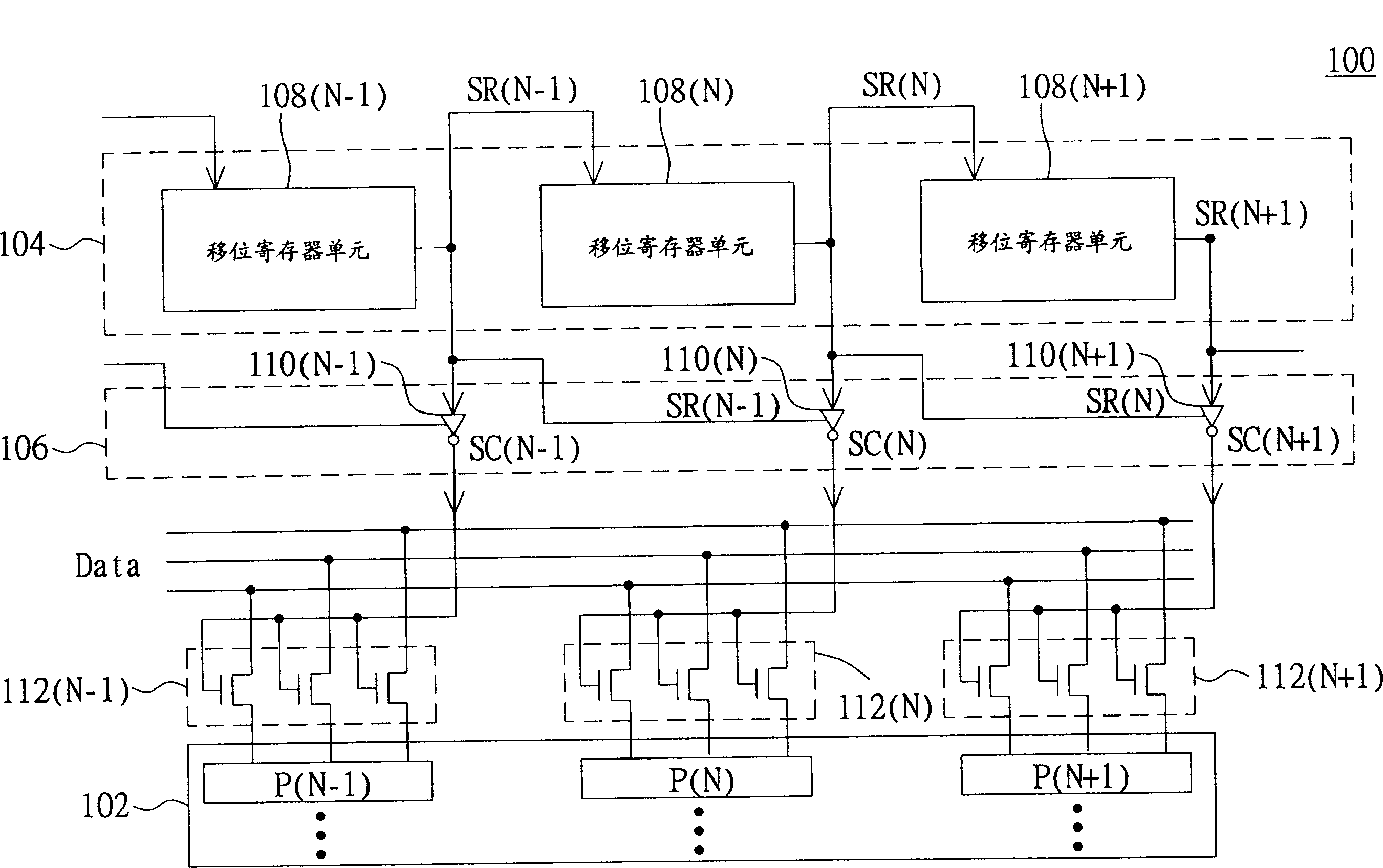
[0021] Please refer to figure 1 , which represents a circuit diagram of a driving circuit according to a first embodiment of the present invention. The driving circuit 100 is used for driving a pixel array 102 of a display panel. The driving circuit 100 at least includes a shift register circuit 104 , an output buffer circuit 106 and a plurality of switch groups 112 . The shift register circuit 104 includes a plurality of shift register units, such as shift register units 108(N−1), 108(N) and 108(N+1). The output buffer circuit 106 includes a plurality of output buffer units, such as main inverters, including main inverters 110(N−1), 110(N) and 110(N+1).

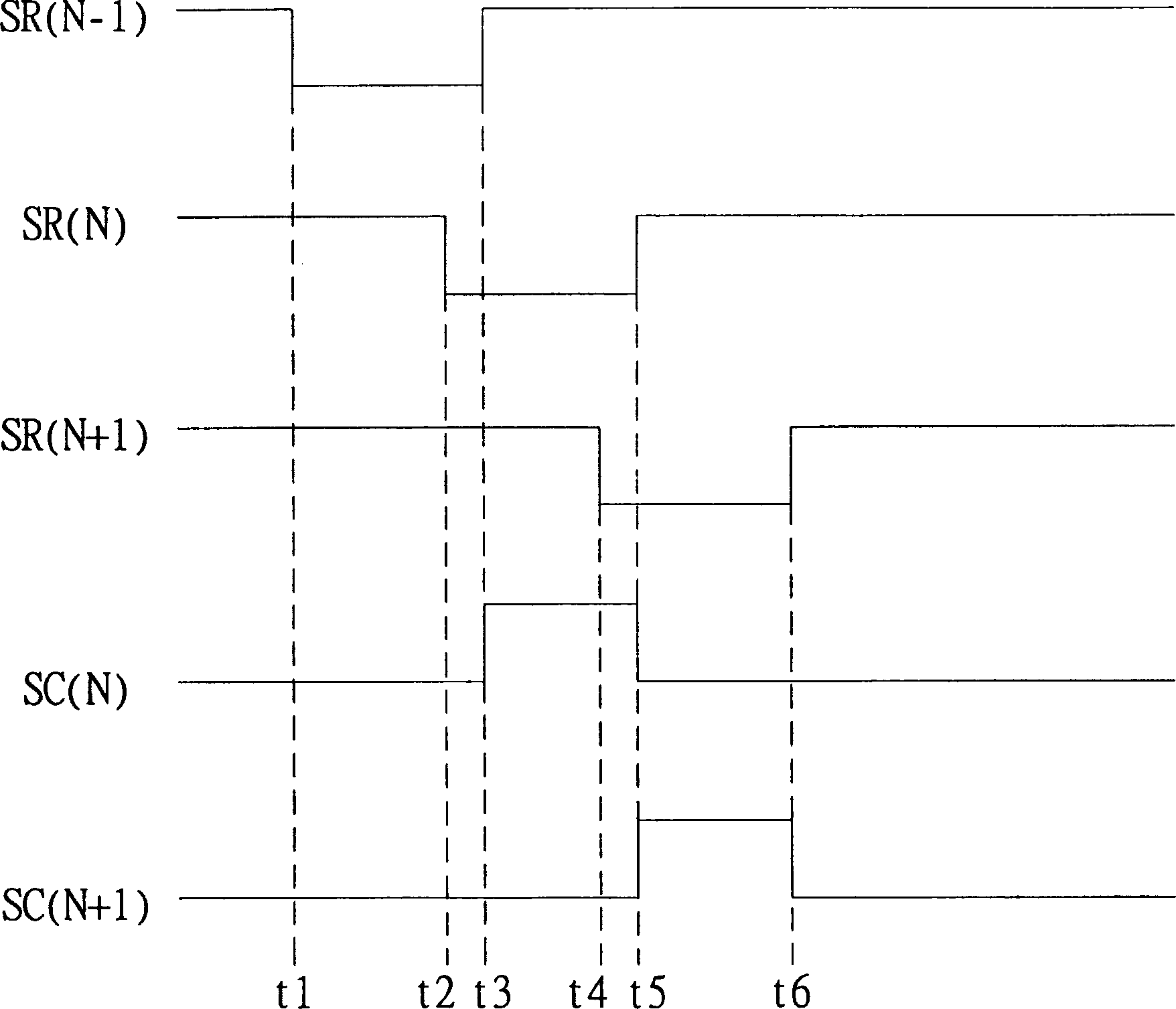
[0022] The shift register units 108(N-1), 108(N) and 108(N) respectively output shift signals SR(N-1), SR(N) and SR(N+1), and the shift signal SR(N -1), SR(N) and SR(N+1) are enabled sequentially. When the shift signals SR(N-1), SR(N) and SR(N+1) are enabled respectively, the levels of the shift signals SR(N-1), SR(N) an...

Embodiment 2

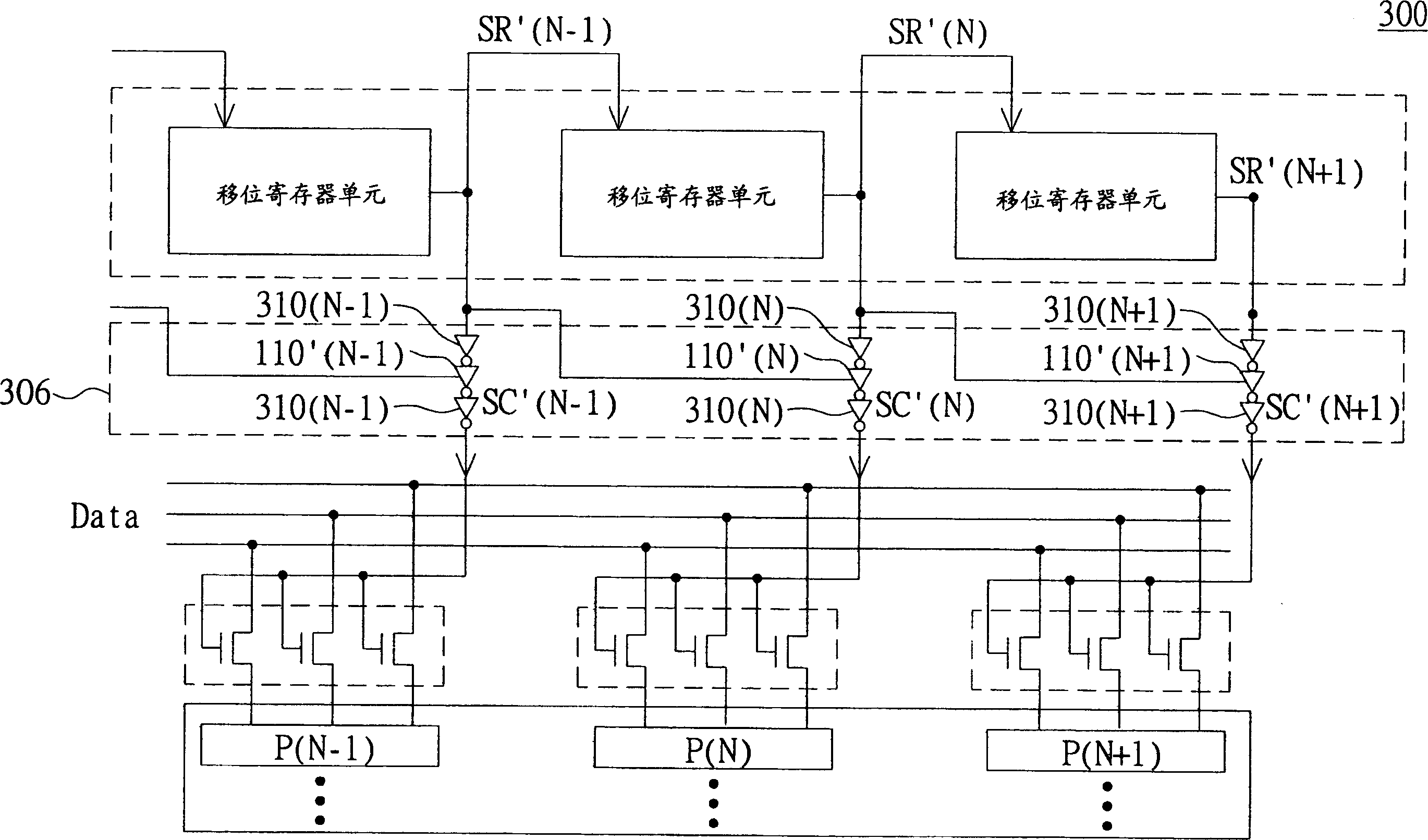
[0029] Please refer to image 3, which represents a circuit diagram of a driving circuit according to a second embodiment of the present invention. Different from the first embodiment, in the driving circuit 300 of the second embodiment of the present invention, the output buffer circuit 306 further includes a plurality of auxiliary inverters 310 (N-1), a plurality of auxiliary inverters 310 ( N) and a plurality of auxiliary inverters 310 (N+1), such as two auxiliary inverters 310 (N-1), two auxiliary inverters 310 (N) and two auxiliary inverters 310 ( N+1). The two auxiliary inverters 310(N-1) are connected in series with the main inverter 110'(N-1), and the two auxiliary inverters 310(N) are connected in series with the main inverter 110'(N). connected, and the two auxiliary inverters 310(N+1) are connected in series with the main inverter 110'(N-1). The positive voltage supply terminals of all auxiliary inverters can receive the shift signal of the upper stage, or be dir...


PUM


Abstract

The driver circuit includes one shift register circuit and one output buffer circuit. The shift register circuit includes the first and the second shift register units to output the first and the second shift signals separately for use successively. The output buffer circuit include the first and the second output buffer units to receive the first and the second shift signals separately to output the first and the second switch controlling signals. The voltage supplying end of the second buffer unit receives the first shift signal. When the first shift signal is in the non-activation level, the second buffer unit is activated, so that the second buffer unit outputs the second switch control signal to output the first data signal the pixel array.

Description

technical field [0001] The present invention relates to a driving circuit, and more particularly to a driving for driving a pixel array of a display panel. Background technique [0002] A general method for driving a pixel array of a thin film transistor (Thin Film Transistor) liquid crystal display panel (Liquid Crystal Display Panel) or an OLED display panel is briefly described as follows. The driving circuit at least includes a horizontal shift register (Horizontal Shift Register), a plurality of switch groups, and a vertical shift register (Vertical Shift Register). The vertical shift register is used to output a plurality of enable vertical shift signals in sequence, so that each column of pixels is enabled in sequence. The horizontal shift register is used for outputting a plurality of horizontal shift signals for respectively controlling a plurality of switch groups. Multiple horizontal shift signals are enabled sequentially, so that multiple switch groups are sequ...

Claims


Application Information

Patent Timeline
IPC IPC(8): G02F1/133G09G3/20G09G3/30G09G3/36H04N5/66
Inventor 陈昶佑尤建盛
Owner AU OPTRONICS CORP
Why Eureka
Try Eureka