Data transfer apparatus

A data transmission device and data transmission technology, which are applied in the fields of electrical digital data processing, television, color television, etc., can solve the problems of low buffer usage efficiency, low access frequency, and inability to perform high-speed access, and reduce buffering. The effect of the device capacity

Inactive Publication Date: 2005-06-08
PANASONIC CORP
View PDF1 Cites 7 Cited by
  • Summary
  • Abstract
  • Description
  • Claims
  • Application Information

AI Technical Summary

Problems solved by technology

[0014] First, because each functional processing device has a buffer structure, the scale of hardware is too large
In addition, when the transfer unit from a specific function processing device to the buffer becomes the number of words that is lower than the capacity of the buffer, or the access frequency becomes low, the use efficiency of the specific buffer becomes low.
[0015] The 2nd, because in the data transmission between a plurality of functional processing devices and the shared memory accessed from a plurality of functional processing devices, data transmission must be performed via a buffer, so extra consumption is generated when accessing, and I cannot perform high-speed access

Method used


Image

  • Data transfer apparatus
  • Data transfer apparatus
  • Data transfer apparatus

Examples


Embodiment 1

[0062] Next, Embodiment 1 of the present invention will be described using the drawings.

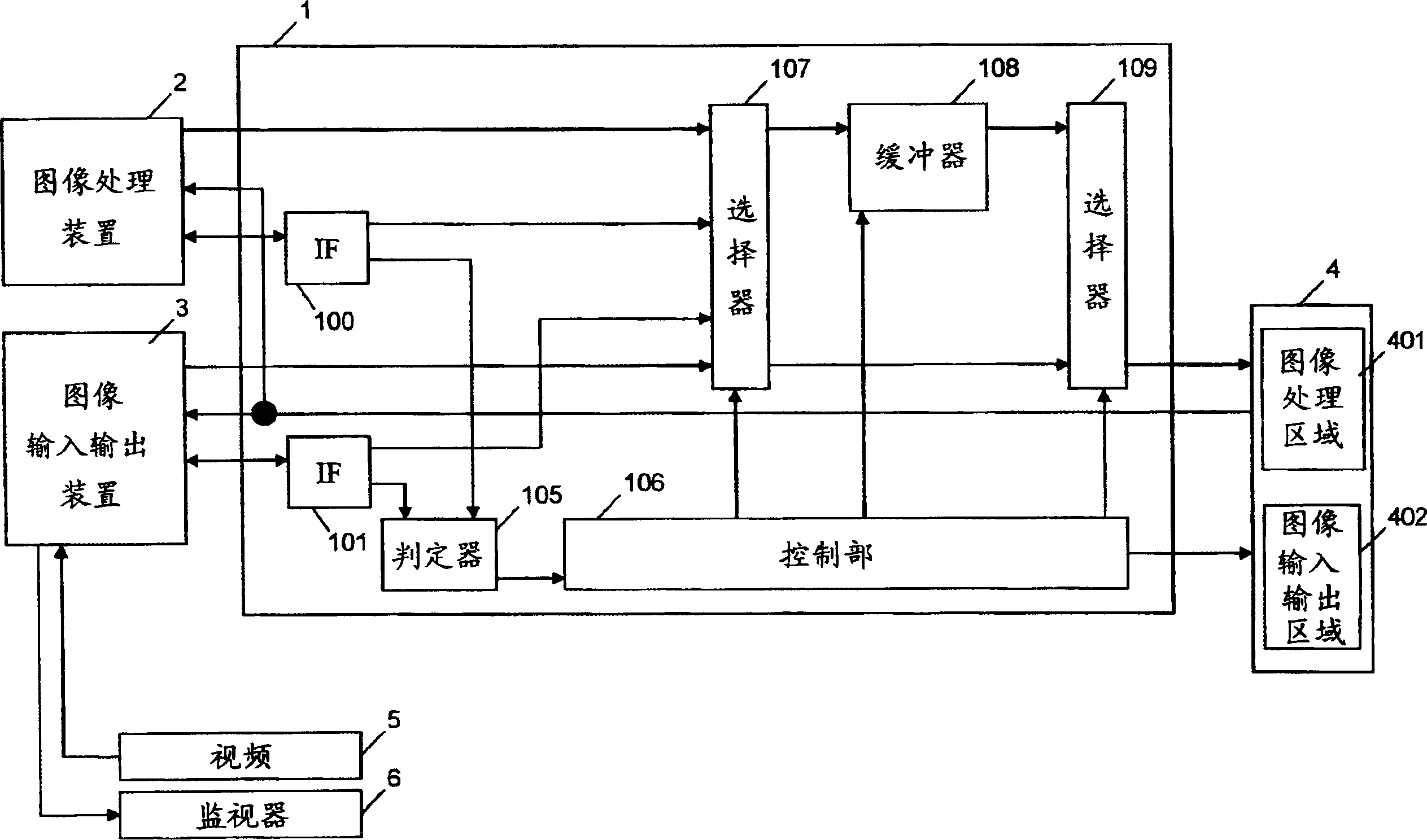
[0063] figure 1 is a block diagram showing the structure of the data transmission device according to Embodiment 1 of the present invention.

[0064] exist figure 1 Among them, symbols 2 to 6 are the same functional blocks as those in the prior art. In the data transmission device 1 , the interface 100 performs data transmission control with the image processing device 2 . The interface 101 performs data transfer control with the image input / output device 3 . The selector 107 makes the transmission data from the image processing device 2 and the transmission control signal from the interface 100 a first input, makes the transmission data from the image input and output device 3 and a transmission control signal from the interface 101 a second input, and controls The control signal of the unit 106 selects and outputs the above-mentioned transmission data to the buffer 108 and the se...

Embodiment 2

[0079] use Figure 10 and Figure 11 The data transmission sequence in the data transmission device according to Embodiment 2 of the present invention will be described. Figure 10 and Figure 11 A case where read transfer is performed by the image processing device 2 while burst transfer is performed by the image input / output device 3 is shown. Figure 10 Represents the data transmission timing in the data transmission device of the prior art, Figure 11 The sequence of data transmission in the data transmission device according to the second embodiment of the present invention is shown. The structure of the data transmission device is the same as that of Embodiment 1.

[0080] In the prior art data transmission device, in Figure 10 , the image input / output device 3 starts the transfer to the shared memory 4 with a burst transfer. During the burst transfer, the image processing device 2 outputs a read request to the shared memory 4 . The data D10 to D14 from the image...

Embodiment 3

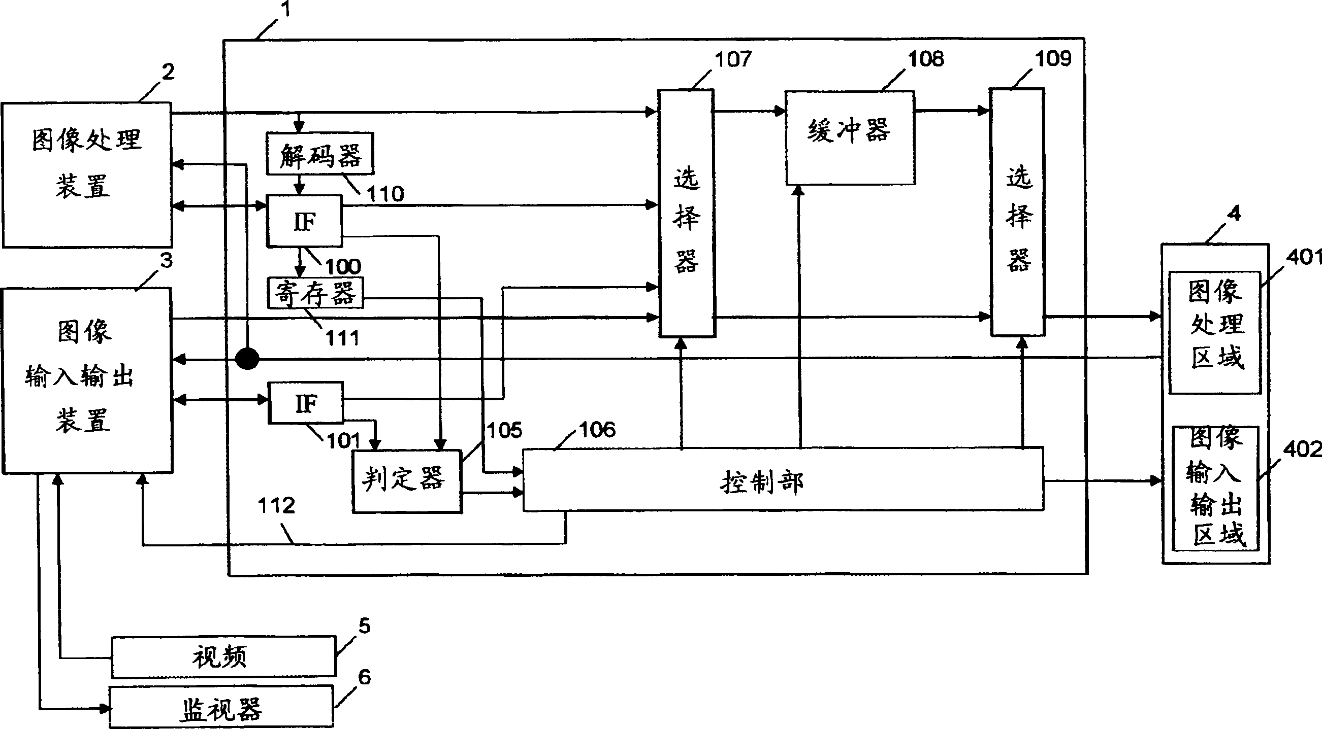
[0085] figure 2 is a block diagram showing the configuration of a data transmission device according to Embodiment 3 of the present invention.

[0086] exist figure 2 Among them, symbol 110 denotes an address decoder, symbol 111 denotes a buffer transfer request register, and symbol 112 denotes a buffer transfer end notification interrupt signal. For other structural elements with figure 1 same function.

[0087] Seen from the image processing device 2 , the data transfer device 1 is mapped to an address to the shared memory 4 and an address to the buffer transfer request register 111 . Then, an access address from the image processing device 2 is decoded by the address decoder 110 to access the buffer transfer request register 111 . When the access to the buffer transfer request register 111 is started, the control unit 106 starts transferring the data held in the buffer 108 to the shared memory 4, and the control interface keeps the buffer transfer request register ac...


PUM


Abstract

The present invention provides a buffer between the image processing device, the image input / output device, and a shared memory shared and accessed by them, controls the use of the buffer only for a specific access, and controls data transfer to the shared memory. For a single transfer request from the image processing device and a burst transfer request from the image input-output device, a single transfer data is held in the buffer, and the selector is controlled so as to perform burst transfer to the memory.

Description

technical field [0001] The present invention relates to a data transmission device, and more particularly to a data transmission device capable of handling data transmission between a plurality of functional processing devices and shared resources shared and accessed by a plurality of functional processing devices with less hardware. Background technique [0002] In addition to performing data processing, it is used in various systems as a system in which a plurality of functional processing devices access a common resource. [0003] As a first example, there is a graphics system that shares a frame memory. In this graphics system, there are cases where the rendering processing device writes image bitmap data into a specific area of ​​the frame memory, and the video controller periodically reads out the frame memory. In this case, the rendering processing device performs image generation processing for expressing a so-called line or polygonal object. T...

Claims


Application Information

Patent Timeline
Patent Type & Authority Applications(China)
IPC IPC(8): G06T1/60G06F13/38H04J3/26H04N5/00H04N21/458
CPCH04N21/4583
Inventor 川口谦一三野吉辉
Owner PANASONIC CORP
Why Eureka
Try Eureka