Electro-optical device and electronic apparatus

An electro-optical device and main power supply technology, which is applied in the direction of electric light sources, identification devices, lighting devices, etc., and can solve the problem of brightness decrease in the central part

Active Publication Date: 2005-07-27
SEIKO EPSON CORP
View PDF1 Cites 27 Cited by
  • Summary
  • Abstract
  • Description
  • Claims
  • Application Information

AI Technical Summary

Problems solved by technology

Therefore, for Figure 17 In the up and down directions shown, there is a problem such as a decrease in the brightness of the central part

Method used


Image

  • Electro-optical device and electronic apparatus
  • Electro-optical device and electronic apparatus
  • Electro-optical device and electronic apparatus

Examples


no. 1 approach

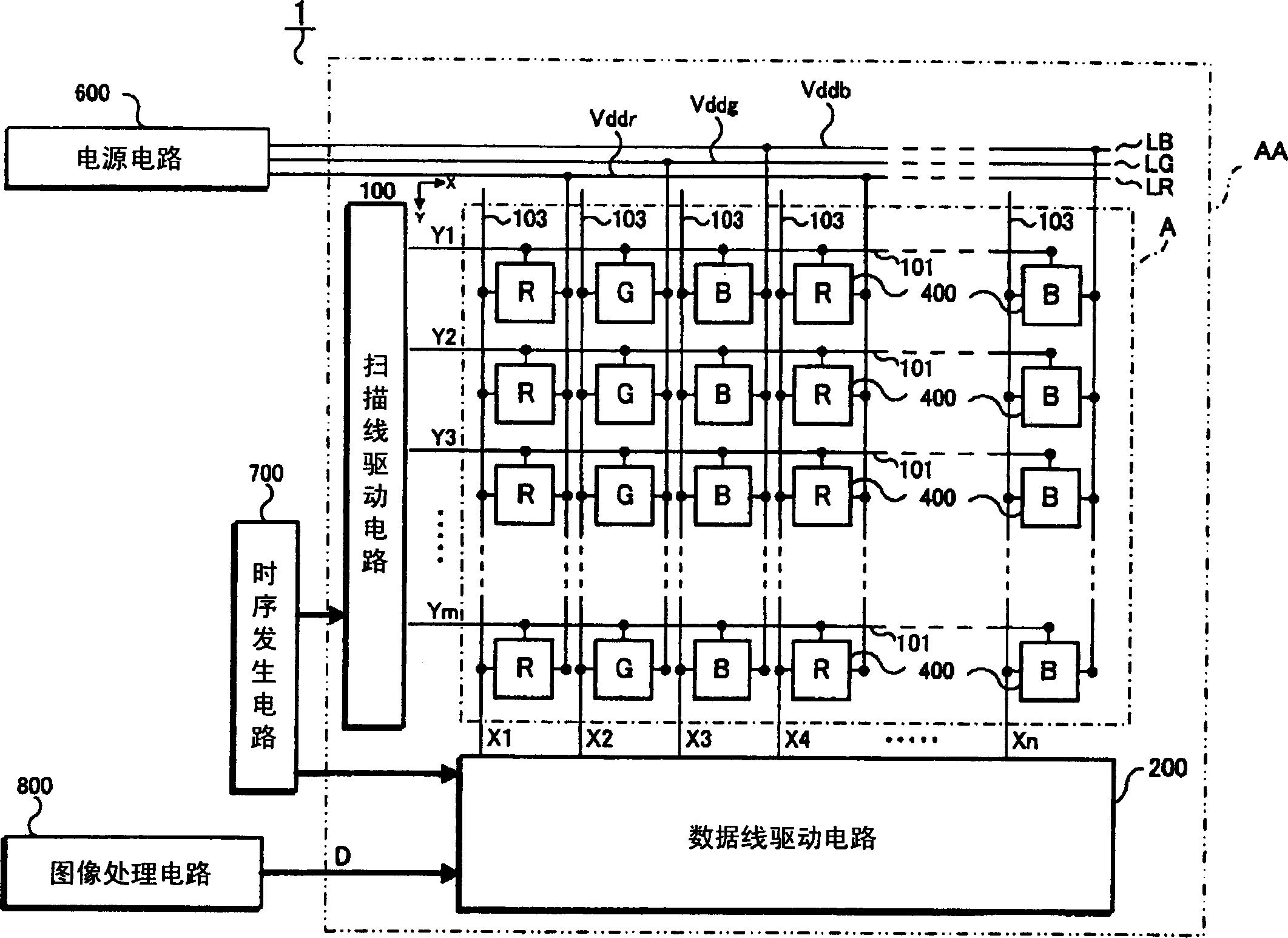
[0039] figure 1 It is a block diagram showing a schematic configuration of the electro-optical device according to the first embodiment of the present invention.

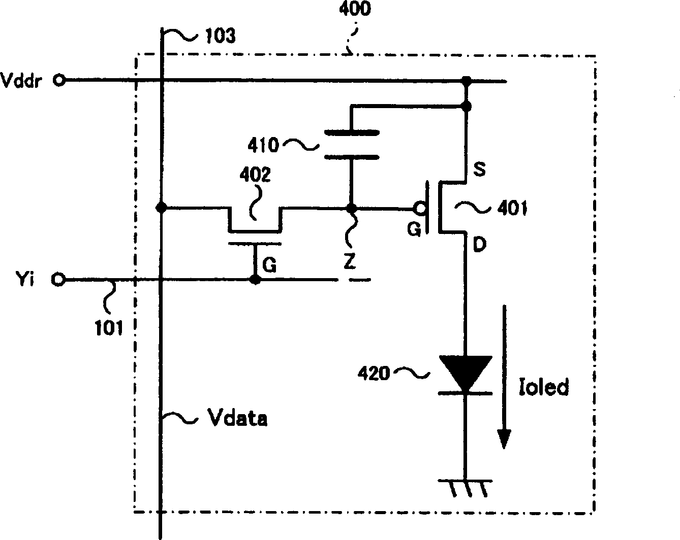
[0040] The electro-optical device 1 includes an electro-optical panel AA and external circuits. A pixel region A, a scanning line driving circuit 100 and a data line driving circuit 200 are formed on the electro-optical panel AA. Wherein, in the pixel area A, m scanning lines 101 parallel to the X direction are formed, and n data lines 103 parallel to the Y direction are formed, and the Y direction is perpendicular to the X direction. Pixel circuits 400 are respectively provided corresponding to intersection points of the scanning lines 101 and the data lines 103 . The pixel circuit 400 includes an OLED element. The symbols "R", "G" and "B" shown in the figure indicate the emission color of the OLED element. In this example, pixel circuits 400 of various colors are arranged along the data line 103 .

[0041] A...

no. 2 approach

[0052] Next, an electro-optical device 1 according to a second embodiment will be described. The electro-optical device 1 of the second embodiment has the same configuration as that of the electro-optical device 1 of the first embodiment, except that the power wiring of the same power supply voltage is commonly used for the R color and the B color. Although the electro-optical device 1 of the first embodiment presupposes that the luminous efficiency of the OLED element 420 differs for each luminous color, depending on the type of organic EL material used for the luminescent layer, the luminous efficiency is similar even if the luminous color is different. type of material. The electro-optical device 1 of the second embodiment is a device using, for example, an OLED element 420 having similar luminous efficiencies in R color and B color. As for color matching, those colors having similar voltage values ​​when displaying white are matched with each other. For example, when the...

no. 3 approach

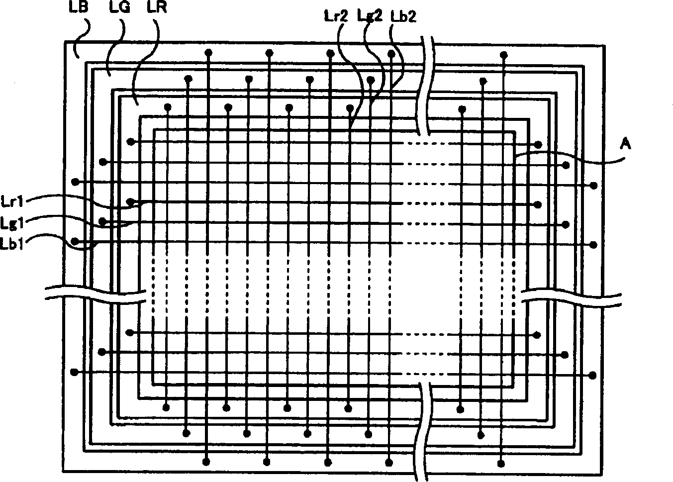
[0060] Next, an electro-optical device 1 according to a third embodiment will be described. The electro-optical device 1 of the third embodiment differs from the electro-optical device 1 of the first embodiment in using a monochromatic OLED element. Image 6 Indicates the detailed structure of power wiring. In this case, since one type of power supply voltage is sufficient, the main power supply line constitutes only LW shown in the figure. Auxiliary power supply connection points P are all provided at locations corresponding to intersections of the first auxiliary power supply line Lw1 and the second auxiliary power supply line Lw2 . That is, the first auxiliary power supply line Lw1 and the second auxiliary power supply line Lw2 are arranged in a grid pattern, and the power supply impedance is significantly reduced by connecting them at these intersections. Therefore, a uniform power supply voltage can be supplied to each pixel circuit 400 .

[0061] However, the power su...


PUM


Abstract

The improvement of brightness unevenness. A plurality of pixel circuits 400 is arranged in a pixel region A. Main power lines LR, LG, and LB are provided in the outside of the pixel region A. In addition, first sub-power lines Lr1, Lg1, and Lb1 and second sub-power lines Lr2, Lg2, and Lb2 are provided in the inside of the pixel region A so as to be connected to each other at sub-power line connecting points P. Further, the pixel circuits 400 are connected to the first sub-power lines Lr1, Lg1, and Lb1 at pixel connecting points Q. The structure in which these power lines are arranged in a mesh shape enables a considerable reduction in voltage drop and the improvement of brightness unevenness.

Description

technical field [0001] The present invention relates to an electro-optical device equipped with a self-luminous element and an electronic device using the same. Background technique [0002] In recent years, devices incorporating organic light-emitting diodes (hereinafter referred to as OLED elements) have attracted attention as image display devices instead of liquid crystal display devices. An OLED (Organic Light Emitting Diode: Organic Light Emitting Diode) element is a current-driven self-luminous element that emits light by itself, unlike a liquid crystal element that changes the amount of light transmitted. [0003] In an electro-optical device driven by an active matrix using an OLED element, a pixel circuit for adjusting gradation of light emission is provided to the OLED element. The setting of the luminous gray scale in each pixel circuit is realized by providing the pixel circuit with a voltage value or a current value corresponding to the luminous gray scale to ...

Claims


Application Information

Patent Timeline
Patent Type & Authority Applications(China)
IPC IPC(8): H05B33/12G09F9/30G09G3/30G09G3/32H01L27/32H01L51/50H05B33/06H05B33/14
CPCG09G2300/0465G09G2300/0842H01L27/3276G09G2300/0452G09G2320/0242G09G3/3233G09G2330/02G09G2320/0223G09G2300/0426H01L27/3211H10K59/35H10K59/131G09G3/30
Inventor 神田荣二
Owner SEIKO EPSON CORP
Why Eureka
Try Eureka