Method for implementing semiconductor laser lightbeam shaping by off-axis all internal reflecting prism array

A total internal reflection prism and beam shaping technology, applied in the field of laser technology applications, can solve problems such as reduced efficiency, achieve cost savings and reduce adjustment difficulty

Inactive Publication Date: 2005-08-10
INST OF OPTICS & ELECTRONICS - CHINESE ACAD OF SCI
View PDF0 Cites 13 Cited by
  • Summary
  • Abstract
  • Description
  • Claims
  • Application Information

AI Technical Summary

Problems solved by technology

On the one hand, this technology deflects the optical path to form a non-coaxial optical path. On the other hand, every part of the light spot must be reflected during the reflection process, and the efficiency will be reduced.

Method used


Image

  • Method for implementing semiconductor laser lightbeam shaping by off-axis all internal reflecting prism array
  • Method for implementing semiconductor laser lightbeam shaping by off-axis all internal reflecting prism array
  • Method for implementing semiconductor laser lightbeam shaping by off-axis all internal reflecting prism array

Examples


Embodiment 1

[0021] Example 1, the beam is folded 5 times.

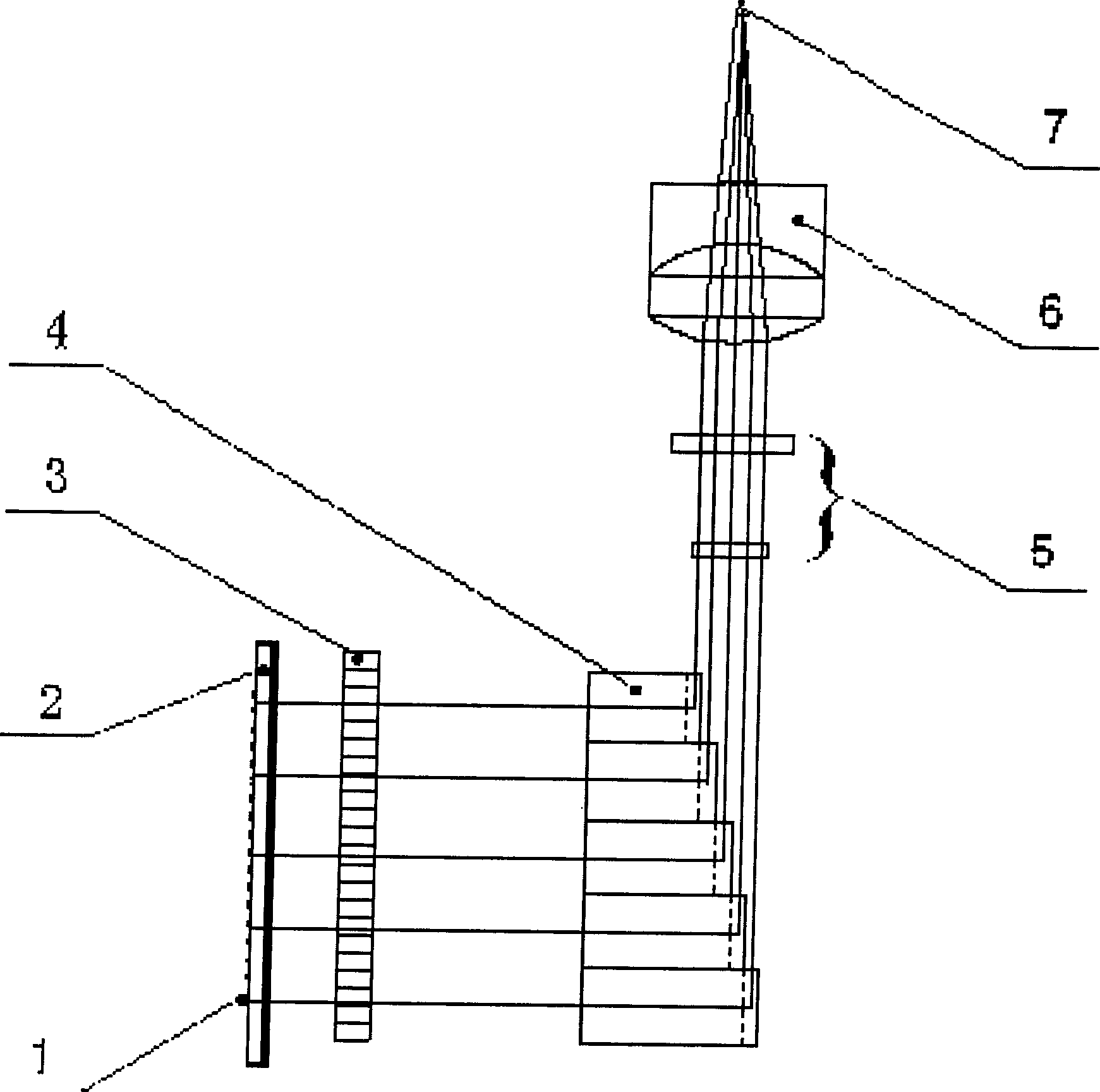
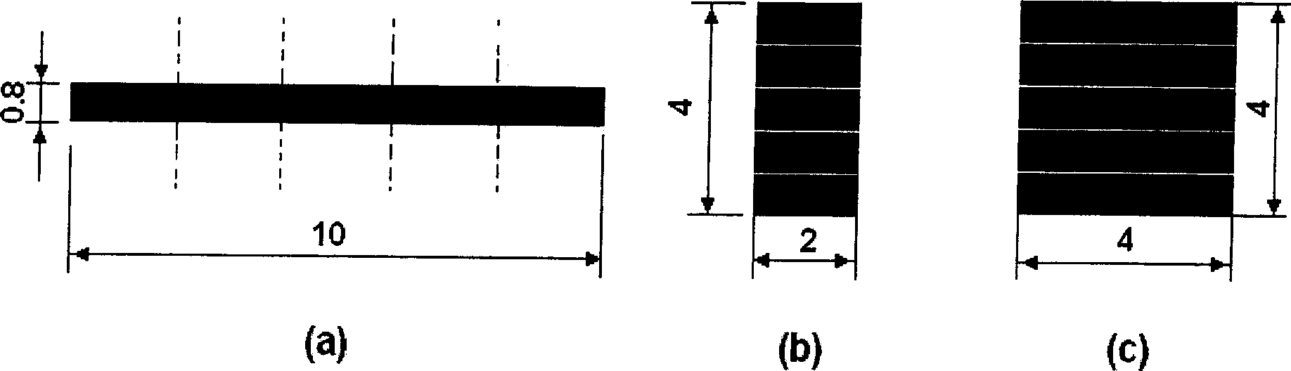
[0022] (1) if figure 1 As shown, the strip semiconductor laser forms a 10mm×0.8mm linear spot with a divergence angle of 0.2°×2.4° after being collimated by the microlens array along the fast and slow axes. The thickness of each reflective prism in the array should be 2mm, and the number of microreflectors should be 5.

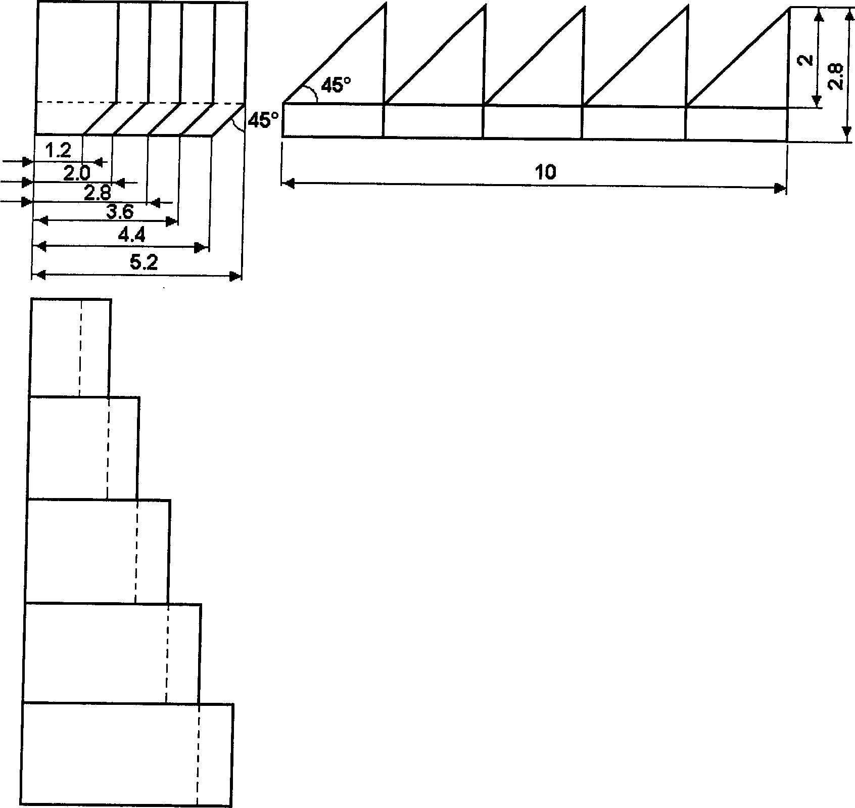
[0023] (2) According to the needs of shaping and folding times 5 times, the thickness of each reflective prism in the shaping micromirror array should be 2mm, the length of two right-angled sides of the prism is 0.8mm, and the displacement of each prism is also 0.8mm, Considering the actual production and adjustment situation, it is designed as figure 2 A shaper composed of five micromirror arrays is shown. The microprisms are individually processed and pressed figure 2 glued together.

[0024] (3) Place the direction correction microreflector group in the optical path of the collimated beam of the semicon...

Embodiment 2

[0028] Example 2, the beam is folded 7 times.

[0029] (1) if Figure 4 As shown, the strip semiconductor laser forms a 10.5mm×0.8mm linear spot with a divergence angle of 0.2°×2.4° after passing through the fast and slow axis collimating microlens array. The thickness of each reflective prism in the microreflective prism array should be 1.5mm, and the total number is 7.

[0030] (2) According to the needs of shaping and folding times 7 times, the thickness of each reflecting prism in the shaping micro-reflecting prism array should be 1.5mm, the length of two right-angled sides of the prism is 0.8mm, and the displacement of each prism is also 0.8mm , taking into account the actual production and adjustment conditions, the design is Figure 5 A shaper composed of five micro-reflecting prism arrays is shown. The microprisms are individually processed and pressed Figure 5 glued together.

[0031] (3) Place the direction correction micro-reflective prism group in the optical...


PUM


Abstract

The present invention relates to a method for implementing semiconductor laser light-beam shaping by utilizing off-axis total internal reflection prism array. It is characterized by that on the optical axis a light beam dividing array formed from reflection prisms with different displacements is adopted. Said invention also provides the concrete steps of said method and concrete structure of said off axis total internal reflection prism array. Said invention can easily implement the conversion of line beam to circular beam or square beam.

Description

technical field [0001] The invention relates to a method for shaping light beams of a semiconductor laser array, belonging to the field of laser technology applications. Background technique [0002] The optical parameter product is an important index to measure the laser beam. The optical parameter product is the product of the diameter of the beam and its far-field divergence angle. When a laser beam is transmitted in a general optical system, the optical parameter product of the beam is constant. Semiconductor lasers are more and more widely used due to their small size, high power, and high electro-optical conversion efficiency. The widely used multi-quantum-well (MQW) semiconductor laser light emission has the following characteristics: First, the geometric size of the semiconductor laser light-emitting cavity is asymmetric, and the horizontal and vertical directions are 100-150 microns and 1 micron, respectively. The field distribution is in the shape of an astigmat...

Claims


Application Information

Patent Timeline
Patent Type & Authority Applications(China)
IPC IPC(8): G02B5/04G02B27/09H01S5/00
Inventor 周崇喜谢伟民郑春燕杜春雷郑国兴杨欢
Owner INST OF OPTICS & ELECTRONICS - CHINESE ACAD OF SCI
Why Eureka
Try Eureka