Multilayer ceramic electronic part, circuit board and method for producing ceramic green sheet used for manufacturing those part and circuit board

一种陶瓷生片、多层陶瓷的技术,应用在多层电路制造、印刷电路制造、电路基板材料等方向,能够解决绝缘层影响、内部电极图形截面形状增加等问题,达到防止堆叠未对准的效果

Inactive Publication Date: 2005-09-07
TDK CORPARATION
View PDF2 Cites 6 Cited by
  • Summary
  • Abstract
  • Description
  • Claims
  • Application Information

AI Technical Summary

Problems solved by technology

However, this method suffers from the problems that the thickness of the insulating layer (or resolution or diffraction characteristics) affects the cross-sectional shape of the internal electrode pattern and increases the number of process steps
Also, in this method, there are limitations to resolving at high aspect and fabricating thick layers in the case of applying photosensitive pastes and electrodepositing photosensitive powders due to resolution dependence

Method used


Image

  • Multilayer ceramic electronic part, circuit board and method for producing ceramic green sheet used for manufacturing those part and circuit board
  • Multilayer ceramic electronic part, circuit board and method for producing ceramic green sheet used for manufacturing those part and circuit board
  • Multilayer ceramic electronic part, circuit board and method for producing ceramic green sheet used for manufacturing those part and circuit board

Examples


Embodiment 1

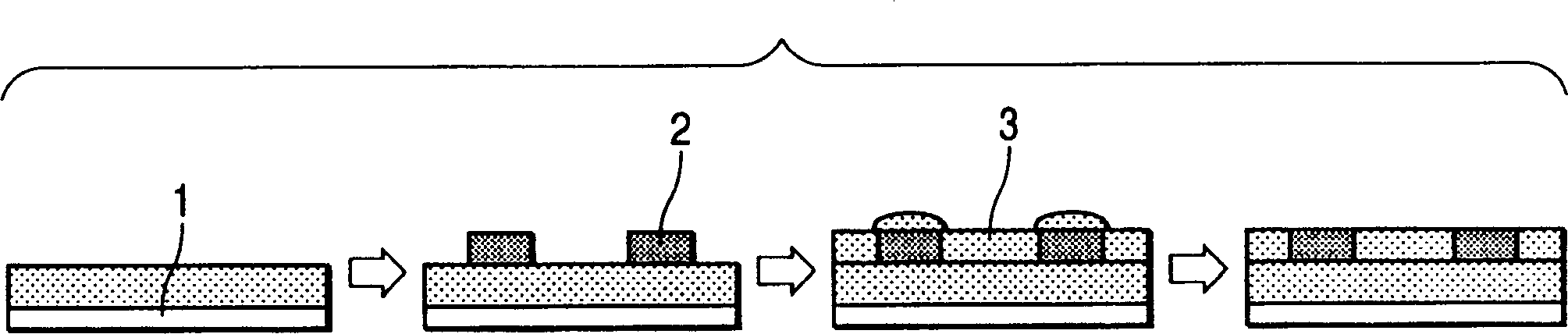
[0040] Such as figure 1 As shown, internal electrodes 2 having a predetermined thickness are formed on substrate 1 by an arbitrary process. A paste of photosensitive ceramic 3 is then applied on the internal electrode surfaces. The paste is dried so that its thickness is substantially equal to that of the internal electrodes just before exposure. Subsequently, after passing the Figure 4 While masking the internal electrode pattern with the photomask 4 shown, the photosensitive ceramic paste is irradiated with light from the upper side of the substrate for exposure. In this process, the surface of the photosensitive ceramic paste is selectively cured while controlling the exposure amount in such a manner that the exposed portion on the surface of the photosensitive ceramic paste is cured. Unexposed portions of the photosensitive ceramic paste are removed by a development process to form a substantially planar layer including internal electrodes.

[0041] By stacking a plur...

Embodiment 2

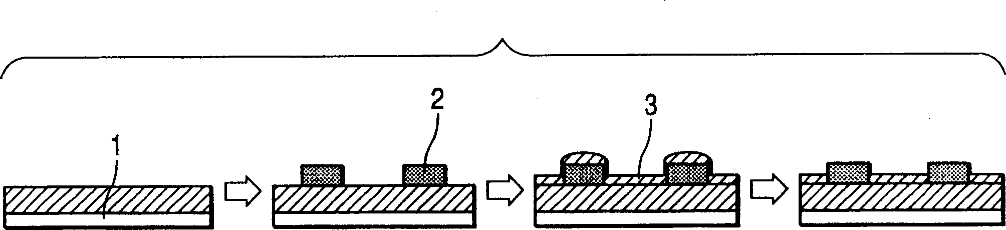
[0045] Such as figure 2 As shown, internal electrodes 2 having a predetermined thickness are formed on substrate 1 by an arbitrary process. The paste of the photosensitive ceramic 3 is then applied on the surface of the internal electrodes. The paste is dried so that its thickness is smaller than that of the internal electrodes just before exposure. Subsequently, after passing the Figure 4 While masking the internal electrode pattern with the photomask 4 shown, the photosensitive ceramic paste is irradiated with light from the upper side of the substrate for exposure. In this process, the surface of the photosensitive ceramic paste is selectively cured while controlling the exposure amount in such a manner that the exposed portion on the surface of the photosensitive ceramic paste is cured. Unexposed portions of the photosensitive ceramic paste are removed through a developing process to expose internal electrode patterns.

[0046] By stacking a plurality of photosensiti...

Embodiment 3

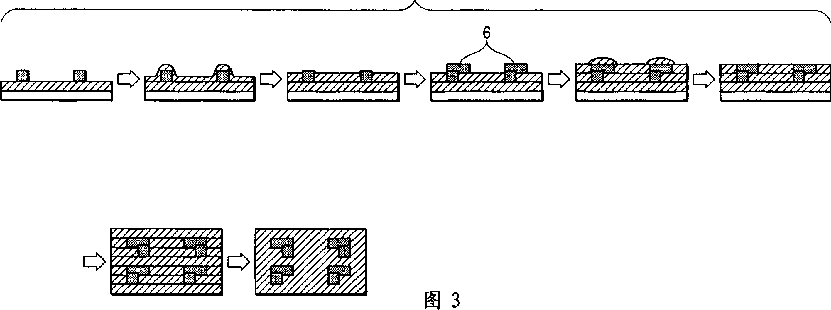
[0048] As shown in FIG. 3, an internal electrode 2 having a predetermined thickness is formed on a substrate 1 by an arbitrary process. The paste of the photosensitive ceramic 3 is then applied on the surface of the internal electrodes. The paste is dried so that its thickness is smaller than that of the internal electrodes just before exposure. Subsequently, after passing the Figure 4 While masking the internal electrode pattern with the photomask 4 shown, the photosensitive ceramic paste is irradiated with light from the upper side of the substrate for exposure. In this process, the surface of the photosensitive ceramic paste is selectively cured while controlling the exposure amount in such a manner that exposed portions on the surface of the photosensitive ceramic paste are cured. Unexposed portions of the photosensitive ceramic paste are removed through a developing process to expose internal electrode patterns. Pattern electrodes 6 are formed on the columnar electrod...


PUM


Abstract

The present invention provides a method for manufacturing an electronic part that can cope with downsizing, improvement in performance and quality of a multilayer electronic part. A ceramic green sheet is produced by forming on a substrate or on a layer formed on a substrate an internal electrode having a predetermined thickness by a discretional process, forming a photosensitive ceramic slurry on a surface of the substrate or the layer and the internal electrode in such a way that its thickness just before exposure will be substantially equal to or smaller than the thickness of the internal electrode from the surface of the substrate or the layer, irradiating the photosensitive ceramic slurry with light from the upper side of the substrate to perform exposure while masking the internal electrode pattern, to selectively harden the surface of the photosensitive ceramic slurry, the exposure amount being controlled in such a way that the surface of the photosensitive ceramic slurry is hardened, and removing the portion of the photosensitive ceramic slurry that has not been exposed by a development process to expose a surface of the internal electrode pattern.

Description

technical field [0001] The present invention relates to a method of manufacturing electronic components exemplified by electronic components composed of so-called multilayer ceramics formed by laminating ceramic green sheets. More specifically, the present invention relates to a method of manufacturing a so-called ceramic green sheet including an electrode layer therein. Examples of the multilayer ceramic electronic parts described here include multilayer ceramic capacitors, multilayer ceramic inductors, LC composite parts including them, and EMC-related parts. Background technique [0002] In recent years, with the miniaturization and rapid spread of electronic devices represented by cellular phones, increased mounting density and improved performance of electronic components for these devices are required. In order to meet these needs, demands for miniaturization and performance improvement achieved by reducing layer thickness and increasing the number of layers are place...

Claims


Application Information

Patent Timeline
Patent Type & Authority Applications(China)
IPC IPC(8): H01G4/12C03B29/00H01F17/00H01F41/04H01G4/00H01G4/30H05K1/03H05K1/09H05K3/00H05K3/06H05K3/46
CPCH01G4/30H05K3/0023H05K3/4667H05K1/0306C04B35/6269H05K2203/0514H05K2201/09881H01G4/12H01F17/00H01F41/04
Inventor 吉田政幸青木俊二须藤纯一渡边源一
Owner TDK CORPARATION
Why Eureka
Try Eureka