Manufacturing method and manufacturing apparatus for image display device

An image display device and a manufacturing method technology, applied in the manufacture of discharge tubes/lamps, ships or lead-in wires, and cold cathode manufacturing, can solve the problems of increasing the withstand voltage to the desired value and achieve withstand voltage characteristics Excellent, display performance and improved reliability

Inactive Publication Date: 2005-09-28
KK TOSHIBA
View PDF3 Cites 2 Cited by
  • Summary
  • Abstract
  • Description
  • Claims
  • Application Information

AI Technical Summary

Problems solved by technology

However, it is difficult to increase the withstand voltage to the desired value only by using such measures, and it is urgent to have more effective measures to improve the withstand voltage

Method used


Image

  • Manufacturing method and manufacturing apparatus for image display device
  • Manufacturing method and manufacturing apparatus for image display device
  • Manufacturing method and manufacturing apparatus for image display device

Examples


Embodiment Construction

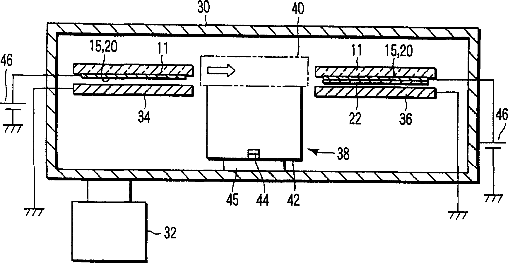
[0041] Hereinafter, a method of manufacturing an image display device and a manufacturing apparatus according to an embodiment of the present invention will be described in detail with reference to the accompanying drawings.

[0042] First, as an image display device manufactured by the method and manufacturing apparatus of the present invention, an FED having a surface conduction type electron emission element will be described as an example.

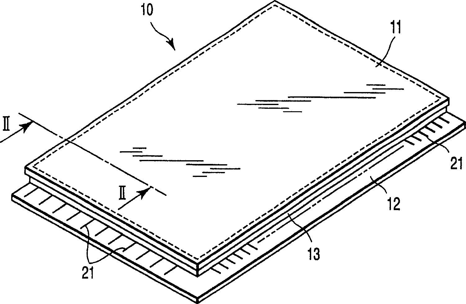
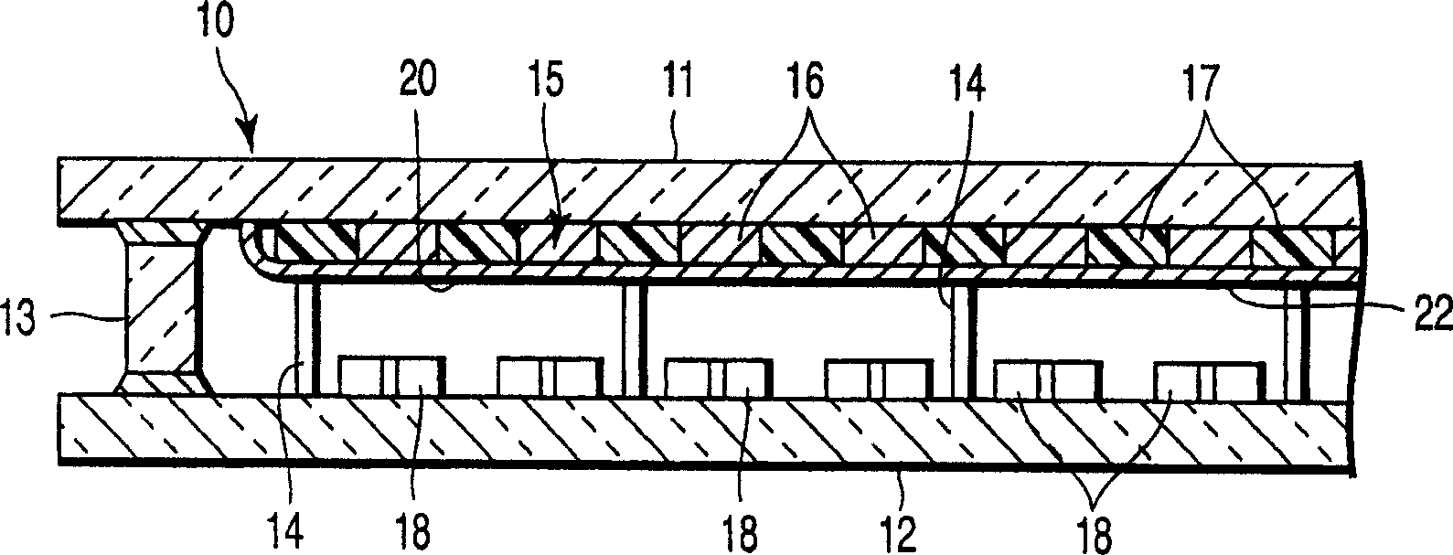
[0043] Such as figure 1 and figure 2 As shown, this FED has, as an insulating substrate, a front substrate 11 and a rear substrate 12 each composed of a rectangular glass plate with a plate thickness of about 1 to 3 mm, and these substrates face each other with a gap of 1 to 2 mm. The front substrate 11 and the rear substrate 12 are connected to each other through the rectangular frame-shaped side wall 13 to form an internal support 10. -4 A flat rectangular vacuum envelope 10 of high vacuum around Pa.

[0044] A plurality of suppo...


PUM


Abstract

At least one substrate of a front substrate (11) or a rear substrate, is opposed to a processing electrode (34, 36) in a vacuum atmosphere, and an electric field is applied between the at least one substrate and the processing electrode, whereby the substrate is electric field-processed. After the electric field processing, the front substrate and the rear substrate kept in the vacuum atmosphere are sealed together to form an envelope.

Description

technical field [0001] The present invention relates to a manufacturing method and manufacturing apparatus of an image display device having a pair of opposing substrates. Background technique [0002] In recent years, as a next-generation image display device, a planar image display device in which a plurality of electron-emitting elements are arranged to face a phosphor surface has been developed and progressed. There are various types of electron emission elements, but most of them use field emission, and display devices using these electron emission elements are generally called field emission displays (hereinafter referred to as FEDs). In FED, a display device using a surface conduction electron emission element is also called a surface conduction electron emission display (hereinafter referred to as SED), but in this application, the term FED is used as a generic term including SED. [0003] The FED generally has a front substrate and a rear substrate facing each othe...

Claims


Application Information

Patent Timeline
Patent Type & Authority Applications(China)
IPC IPC(8): H01J9/24H01J9/26H01J9/38H01J9/385H01J9/40
CPCH01J2217/49H01J9/40H01J9/261H01J9/385H01J9/38H01J9/241
Inventor 小副川政邦小出哲桑原雄二清野和之村田弘贵
Owner KK TOSHIBA
Why Eureka
Try Eureka