Synchronous mirror delay (SMD) circuit and method including a counter and reduced size bi-directional delay line

A delay circuit, delay line technology, applied in digital memory information, instruments, electrical components, etc., can solve problems such as difficulty in obtaining delay resolution

Inactive Publication Date: 2005-09-28
MICRON TECH INC
View PDF0 Cites 6 Cited by
  • Summary
  • Abstract
  • Description
  • Claims
  • Application Information

AI Technical Summary

Problems solved by technology

Additionally, it is difficult to achieve the required delay resolution in SMD 300 due to inherent problems associated with properly sizing the NMOS and PMOS transistors in unit delays 310A-N, as will be appreciated by those skilled in the art
As the frequency of operation increases, even small changes in the variable delay VD can cause undesirable delays or jitter in the CLKSYNC signal relative to the CLK signal

Method used


Image

  • Synchronous mirror delay (SMD) circuit and method including a counter and reduced size bi-directional delay line
  • Synchronous mirror delay (SMD) circuit and method including a counter and reduced size bi-directional delay line
  • Synchronous mirror delay (SMD) circuit and method including a counter and reduced size bi-directional delay line

Examples


Embodiment Construction

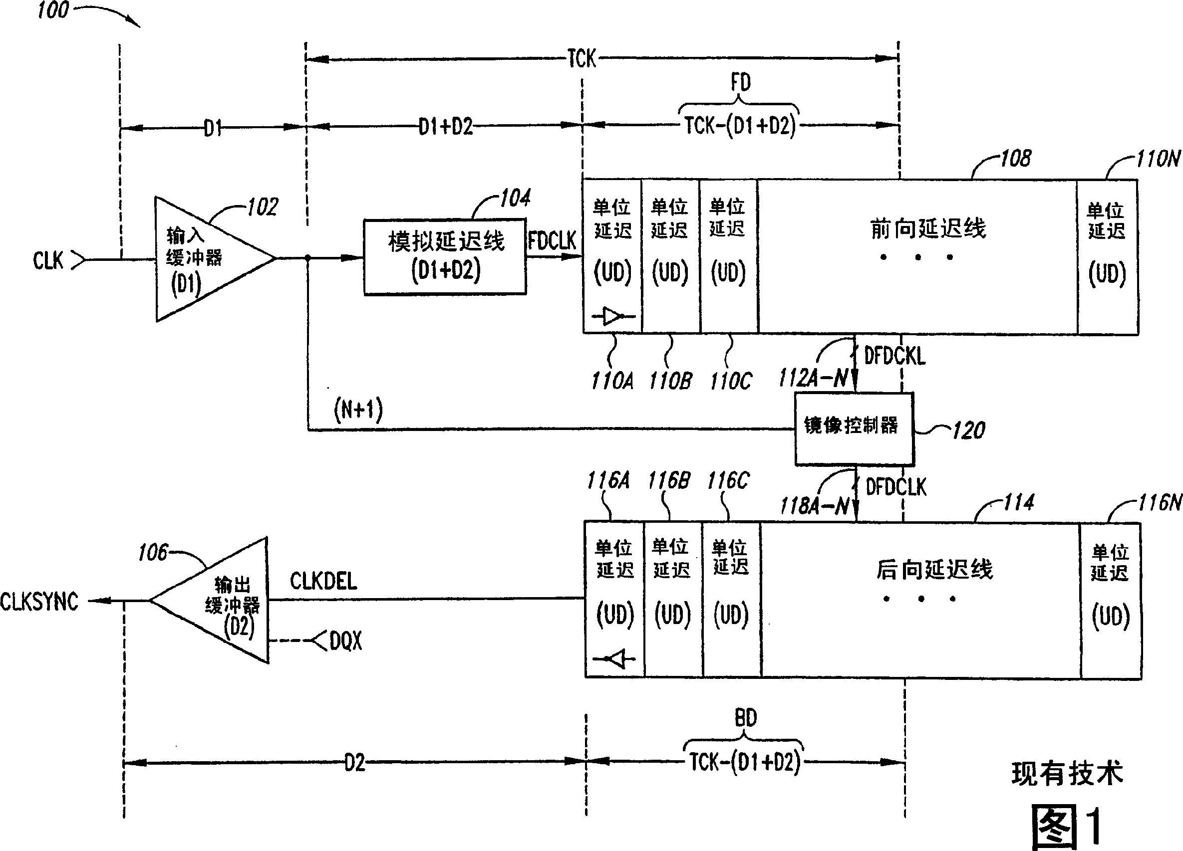
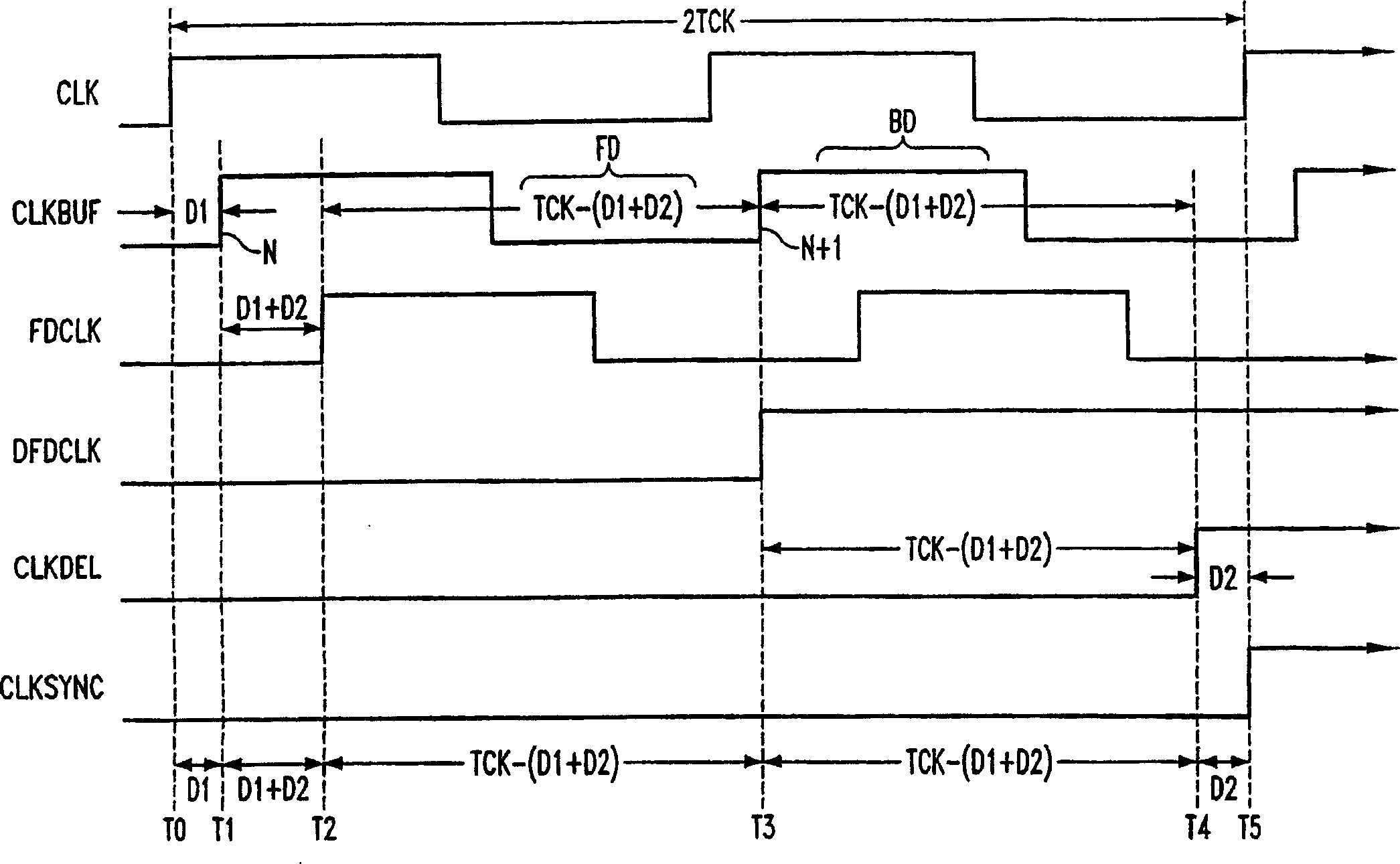
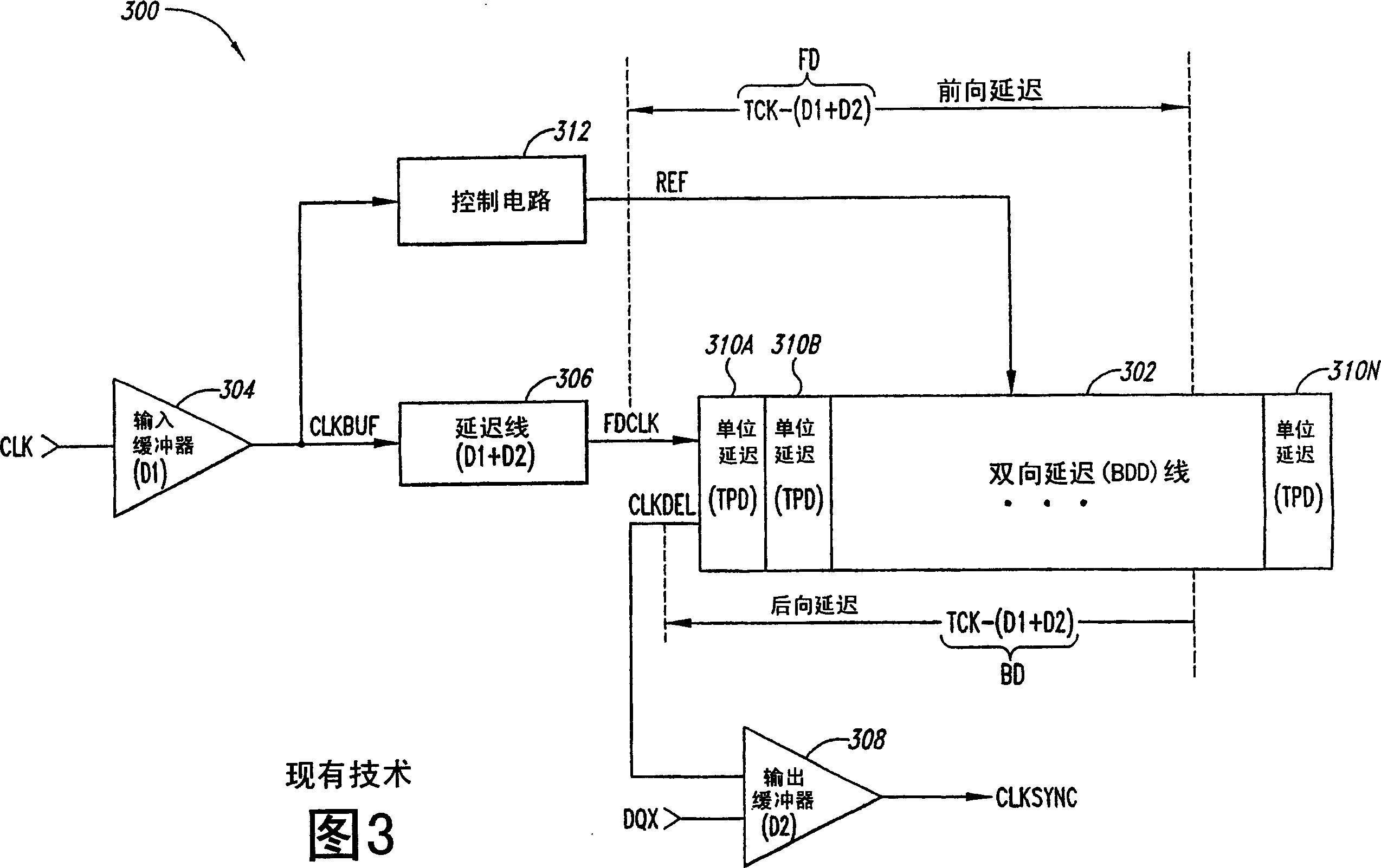
[0045] Figure 6is a functional block diagram depicting an SMD 600 containing a reflective bidirectional delay line 602 comprising a relatively small number of unit delays 604A-H and up / down counters 606 which cooperate to generate a forward delay FD and a backward delay BD are used to generate a synchronous clock signal CLKSYNC which is synchronous with the applied clock signal CLK, as will be described in more detail below. Briefly, delay line 602 operates in a forward delay mode to pass the initial rising edge of forward delayed clock signal FDCLK via unit delays 604A-H in both directions. Meanwhile, each time the signal passes through the first unit delay 604A, the counter 606 increments by one count CNT. Delay line 602 then operates in backward delay mode to reverse the direction of propagation of the rising edge of the FDCLK signal at a given point in time, and thereafter, counter 606 decrements CNT each time the signal passes through the first unit delay, Until the cou...


PUM


Abstract

A synchronous mirror delay (600) includes a model delay line (610) that is coupled to a bi-directional delay line (602). In operation, an initial edge an input clock signal is applied through the model delay line to the bi-directional delay line. The (SMD) thereafter operates in a forward delay mode to alternately operate the bi-directional delay line in a forward mode and a backward mode to propagate the initial edge of the input clock signal through the bi-directional delay line and delay the initial edge of the input clock signal by a forward delay. In response to a subsequent edge of the input clock signal, the SMD mirrors the propagation of the input clock signal through the bi-directional delay line during the forward mode and further delay the initial edge of the input clock signal by a backward delay that is substantially equal to the forward delay.

Description

technical field [0001] The present invention relates generally to integrated circuits, and more particularly to synchronizing an internal clock signal generated in the integrated circuit with an external clock signal applied to the integrated circuit. Background technique [0002] In a synchronous integrated circuit, the integrated circuit is clocked by an external clock signal and performs operations at predetermined times relative to the rising and falling edges of the applied clock signal. Examples of synchronous integrated circuits include synchronous memory devices such as synchronous dynamic random access memory (SDRAM), synchronous static random access memory (SSRAM), and memory cartridges such as SLDRAM and RDRAM, as well as other types of integrated circuits , for example, a microprocessor. The timing of external signals that synchronize memory devices is determined by an external clock signal, and it is often necessary to synchronize operations within the memory d...

Claims


Application Information

Patent Timeline
Patent Type & Authority Applications(China)
IPC IPC(8): G11C7/22H03K5/135H03L7/081
CPCH03L7/0814H03K5/135H03L7/00H03H11/26G11C11/407
Inventor 霍华德·C·基尔希
Owner MICRON TECH INC
Why Eureka
Try Eureka