Stamping system for manufacturing high tolerance parts
A technology of parts and stamping table, applied in the field of stamping process of high-precision tolerance parts, can solve the problem of not providing stamping process and so on
- Summary
- Abstract
- Description
- Claims
- Application Information
AI Technical Summary
Problems solved by technology
Method used
Image

Examples
Embodiment Construction
[0045] The present invention will be described below in conjunction with various embodiments with reference to the accompanying drawings. The present invention has been described in terms of the best mode for achieving the objects of the invention, but various changes can be made by one skilled in the art without departing from the spirit or scope of the invention.
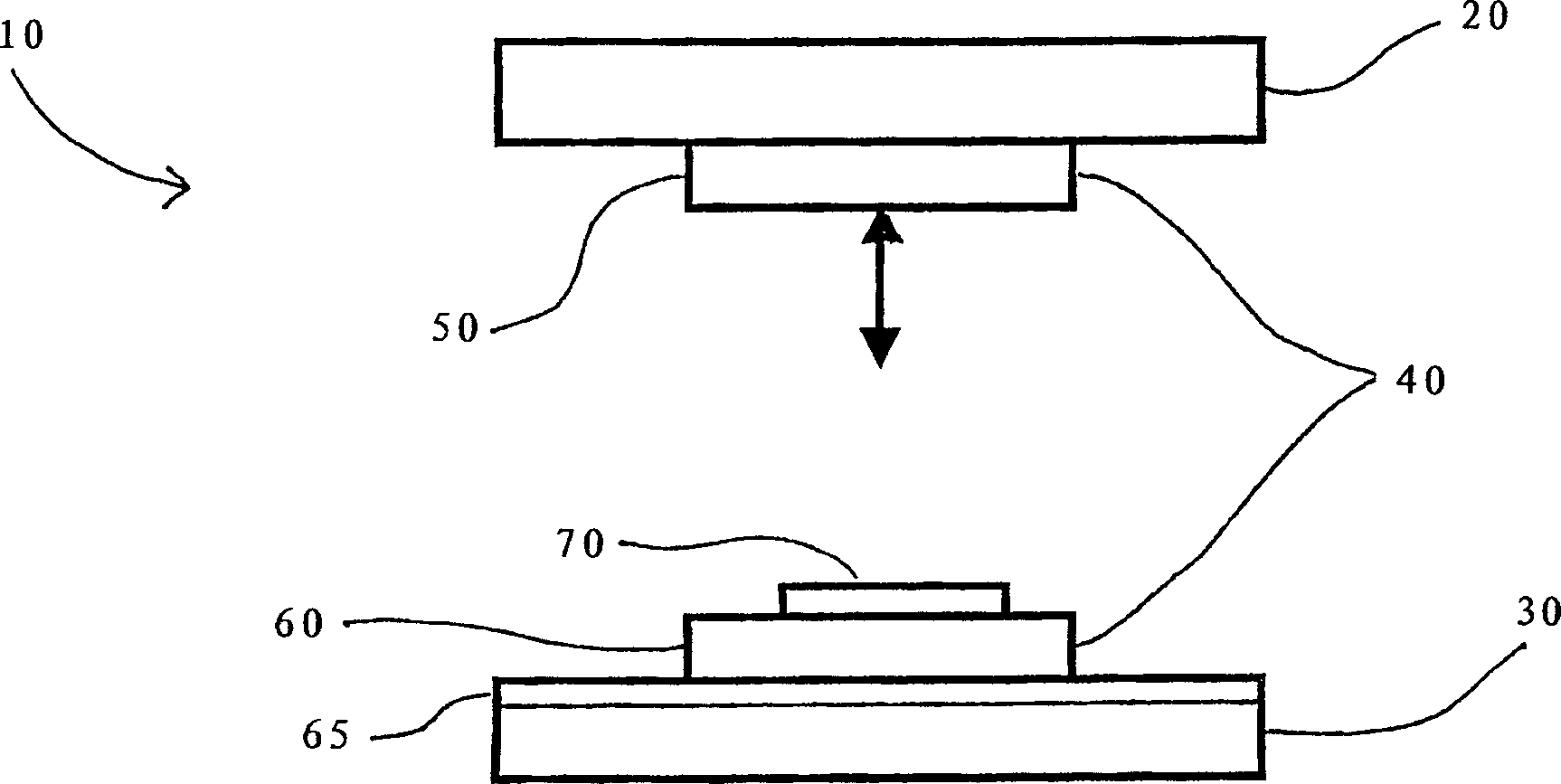
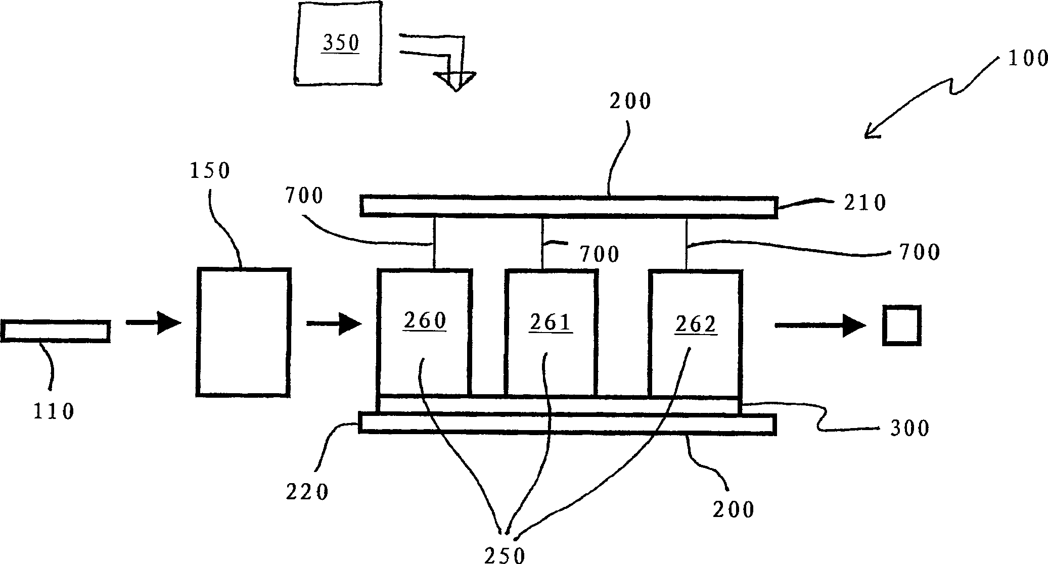
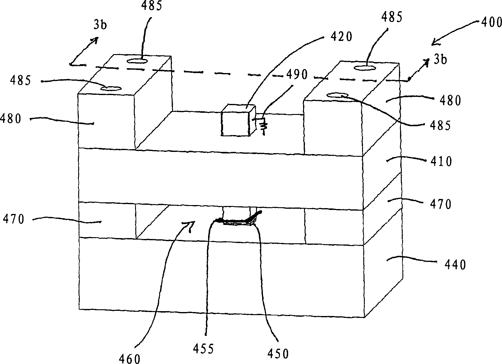
[0046] The present invention relates to a stamping system and method for manufacturing parts with tolerances below 1000nm. The systems and methods of the present invention are particularly suitable for the production of optoelectronic components, including, but not limited to, optoelectronic components, components and subassemblies, active and passive components. To illustrate the principles of the invention, reference is made to an example stamping process for the manufacture of optoelectronic components, particularly fiber optic connectors such as ferrules and slotted ferrules.
[0047] traditional stamping met...
PUM
| Property | Measurement | Unit |
|---|---|---|
| surface roughness | aaaaa | aaaaa |
Abstract
Description
Claims
Application Information