Display device
A technology for display devices and insulating films, applied in lighting devices, electrical components, circuits, etc., can solve the problems of deterioration of transistor characteristics, unclear outline, leakage, etc., and achieve suppression of adverse effects, suppression of adverse effects, and prevention of transistor characteristics worsening effect
- Summary
- Abstract
- Description
- Claims
- Application Information
AI Technical Summary
Problems solved by technology
Method used
Image

Examples
Embodiment approach 1
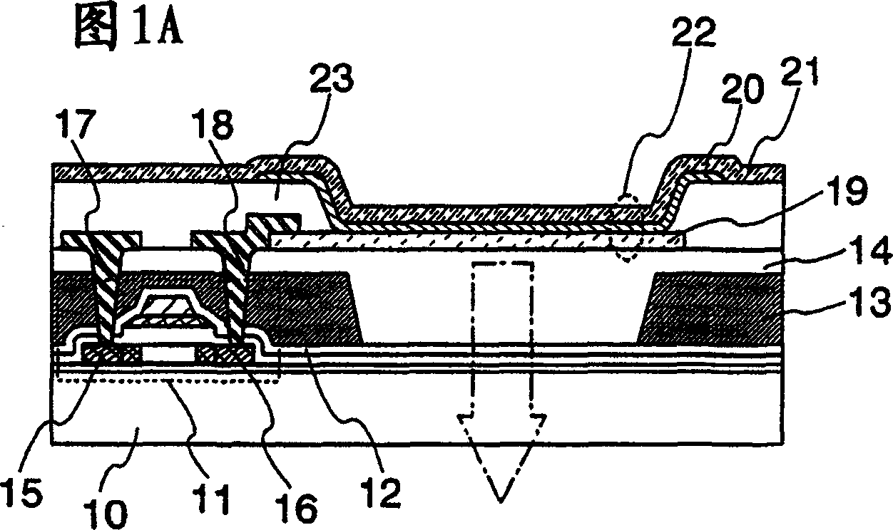
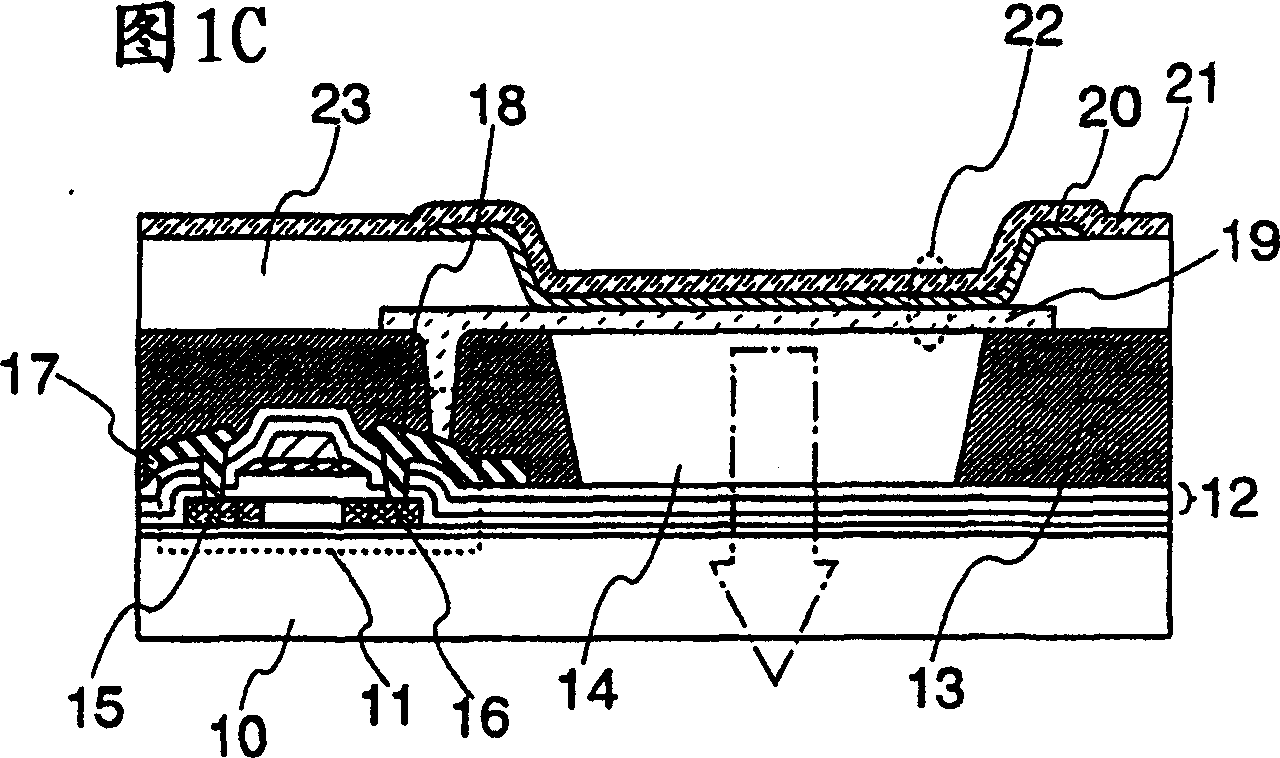
[0033] The cross-sectional structure of the bottom emission type display device according to the present invention, which is roughly divided into four cases, will be described with reference to the accompanying drawings. Further, in this embodiment mode, although it is preferable to form the first insulating film 12 having a barrier property on the transistor as much as possible, it may be omitted. When the first insulating film 12 is omitted in one aspect of the present invention, the "second insulating film 13" and "third insulating film 14" described later should be changed to "the first insulating film 13" and "the third insulating film 14" accordingly. The second insulating film 14".
[0034] The display device of the first structure includes a transistor 11 including source and drain regions 15 and 16 formed over a substrate 10 , a first insulating film 12 formed on the transistor 11 , a first insulating film 12 having a The second insulating film 13 of light shielding ...
Embodiment approach 2
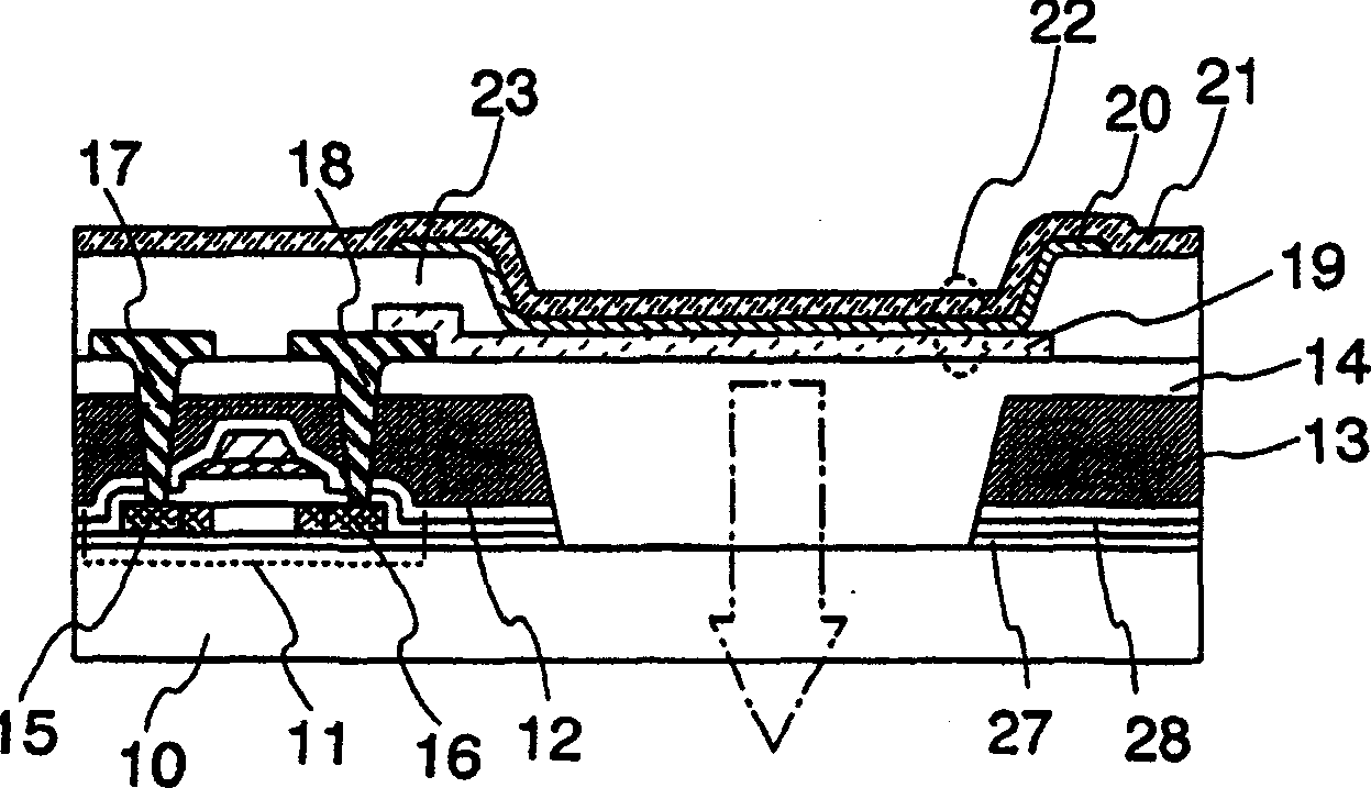
[0067] The cross-sectional structure of the dual emission type display device according to the present invention, which is roughly divided into four cases, will be described with reference to the accompanying drawings. Further, in this embodiment mode, although it is preferable to form the first insulating film 12 having a barrier property on the transistor as much as possible, it may be omitted. When the first insulating film 12 is omitted in one aspect of the present invention, the "second insulating film 13" and "third insulating film 14" described later should be changed to "the first insulating film 13" and "the third insulating film 14" accordingly. The second insulating film 14".
[0068] The display device of the fifth structure includes a transistor 11 formed over a substrate 10, a first insulating film 12 formed over the transistor 11, a second insulating film 13 having a light shielding property formed over the first insulating film 12, A first opening provided in ...
Embodiment approach 1
[0102] The following will refer to Figure 3A and 3B The structure of the display device according to the present invention is described. The display device of the present invention includes a plurality of pixels 310, and each pixel is insulated between the source line Sx (x is a natural number, which satisfies 1≤x≤m) and the gate line Gy (y is a natural number, which satisfies 1≤y≤n) through insulation Multiple components are included in the area where the material intersects (see Figure 3A ). Each pixel 310 includes a light emitting element 313, a capacitive element 316, and two transistors. One of the two transistors is a switching transistor 311 for controlling the video signal input to the pixel 310 , and the other is a driving transistor 312 for controlling ON / OFF of the light emitting element 313 on / off. The capacitive element 316 has a role of holding the gate-source voltage of the transistor 312 . Furthermore, the capacitive element 316 may be eliminated. More sp...
PUM
 Abstract
Description
Claims
Application Information
 - R&D
- Intellectual Property
- Life Sciences
- Materials
- Tech Scout
- Unparalleled Data Quality
- Higher Quality Content
- 60% Fewer Hallucinations
Browse by: Latest US Patents, China's latest patents, Technical Efficacy Thesaurus, Application Domain, Technology Topic, Popular Technical Reports.
© 2025 PatSnap. All rights reserved.Legal|Privacy policy|Modern Slavery Act Transparency Statement|Sitemap|About US| Contact US: help@patsnap.com