Trench MOSFET device with improved on-resistance

A trench and device technology, applied in semiconductor devices, semiconductor/solid-state device manufacturing, electrical components, etc., can solve problems such as increasing the risk of breakdown, increase design and process complexity, reduce on-resistance, reduce The effect of small impedance

Inactive Publication Date: 2005-11-09
GEN SEMICON
View PDF4 Cites 15 Cited by
  • Summary
  • Abstract
  • Description
  • Claims
  • Application Information

AI Technical Summary

Problems solved by technology

However, as a known technique, when the epitaxial layer becomes thinner, the risk of breakdown increases, especially in the termination region which is more susceptible to breakdown

Method used


Image

  • Trench MOSFET device with improved on-resistance
  • Trench MOSFET device with improved on-resistance
  • Trench MOSFET device with improved on-resistance

Examples


Embodiment Construction

[0019] The present invention is described more fully hereinafter with reference to the accompanying drawings, in which preferred embodiments of the invention are shown. This invention may, however, be embodied in various forms and should not be construed as limited to the embodiments set forth herein.

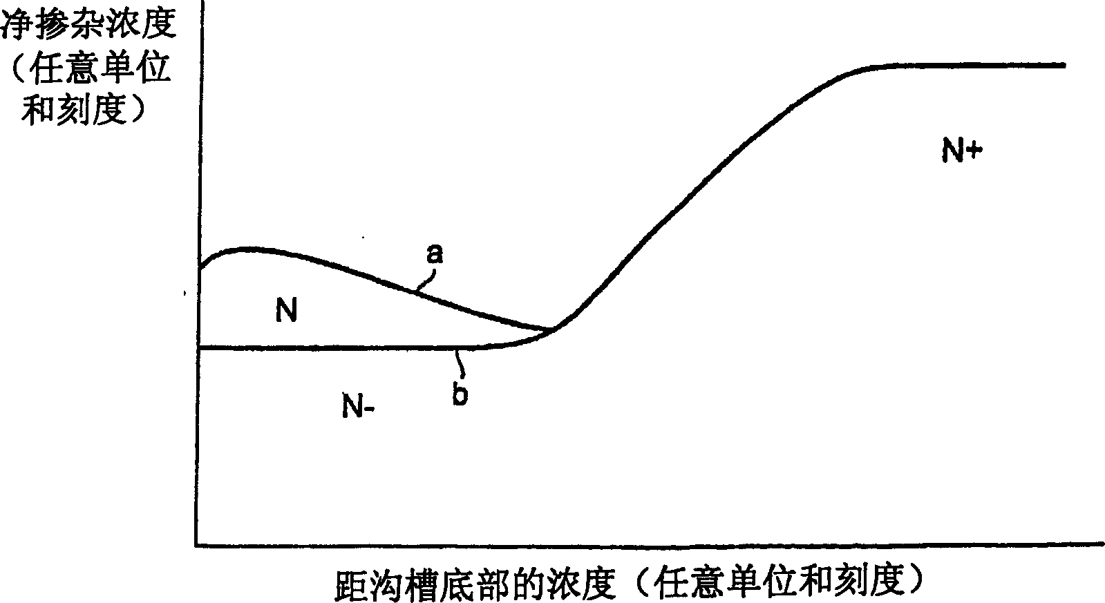
[0020] The present invention relates to new trench MOSFET structures in which a region of higher majority carrier concentration (the preferred mode of formation based on which is sometimes referred to as a "trench bottom implant region") is provided between the bottom of the trench and the substrate. One advantage associated with this trench MOSFET structure is increased on-resistance.

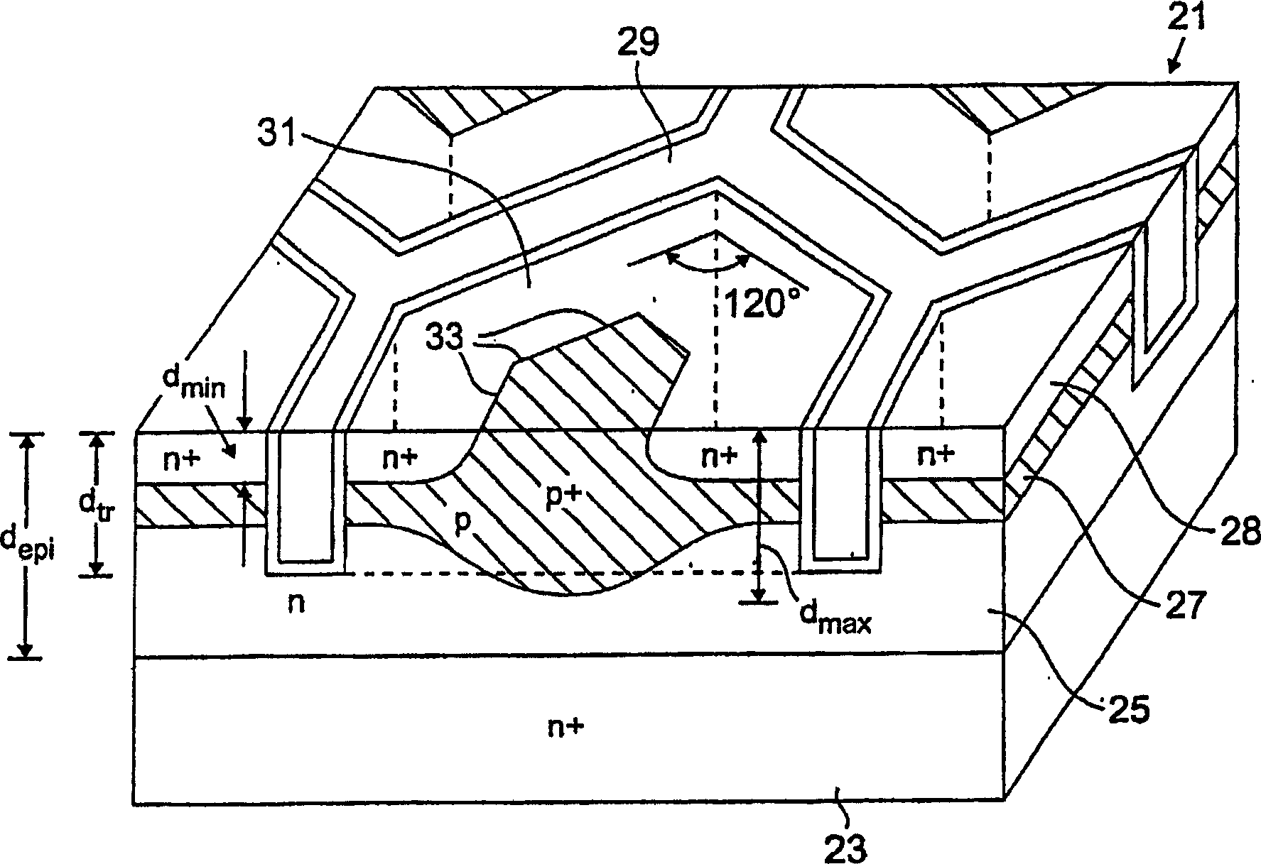
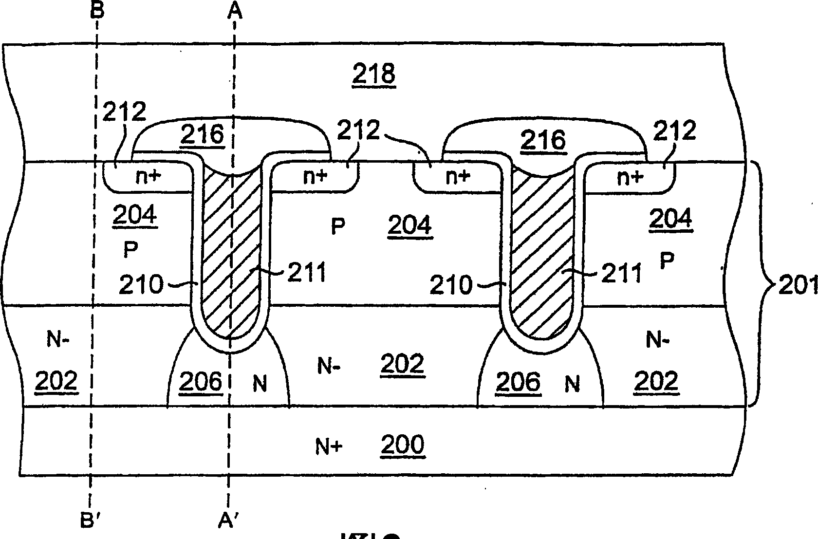
[0021] figure 2 A illustrates a trench MOSFET according to an embodiment of the present invention. In the trench MOSFET shown, an epitaxial layer 201 is provided on an N+ substrate 200 .

[0022] The N+ substrate 200 in this particular example is a silicon substrate, has a thickness in the r...


PUM


Abstract

A trench MOSFET device comprises: a substrate 200 of a first conductivity type, an epitaxial layer of the first conductivity type wherein the epitaxial layer has a lower impurity concentration than the substrate, a trench extending into the epitaxial layer, an insulated conductive region 211 within the trench, a doped region 206 of the first conductivity type formed within the epitaxial layer between a bottom portion of the trench and the substrate, wherein the doped region has an impurity concentration that is lower than that of the substrate and higher than that of the epitaxial layer, a body region 204 of a second conductivity type formed within an upper portion of the epitaxial layer and adjacent trench wherein the body region extends to a lesser depth from the upper surface of the epitaxial layer than does the trench and a source region 212 within the body region.

Description

technical field [0001] The present invention relates to trench MOSFET devices, and more particularly to trench MOSFET devices with increased on-resistance. Background technique [0002] A trench MOSFET (Metal-Oxide-Semiconductor Field-Effect Transistor) is a transistor in which a channel is formed vertically and a gate is formed in a trench extending between a source region and a drain region. A trench lined with a thin insulating layer, such as an oxide layer, and filled with a conductor, such as polysilicon (ie, polysilicon), allows for less compressive current flow and thus provides lower specific on-resistance values. Examples of trench MOSFET transistors are disclosed, for example, in US Pat. Nos. 5,072,266, 5,541,425, and 5,866,931, which are incorporated herein by reference. [0003] As a specific example, FIG. 1 illustrates a half hexagonal trench MOSFET structure 21 disclosed in US Patent No. 5,072,266. The structure includes an n+ substrate 23 on which a predeter...

Claims


Application Information

Patent Timeline
Patent Type & Authority Applications(China)
IPC IPC(8): H01L21/336H01L29/08H01L29/78
CPCH01L29/7813H01L29/0878H01L29/66734H01L21/02521H01L21/0455H01L29/7812H01L2924/13091
Inventor 石甫渊苏根政约翰·E·阿马托崔炎曼
Owner GEN SEMICON
Why Eureka
Try Eureka