Circuit device and manufacturing method thereof

一种电路装置、制造方法的技术,应用在电路装置、电路热装置、印刷电路制造等方向,能够解决难内置发热、装置整体散热性下降、印刷线路板散热性劣化等问题,达到容易搭载的效果

Inactive Publication Date: 2005-12-07
SANYO ELECTRIC CO LTD
View PDF1 Cites 4 Cited by
  • Summary
  • Abstract
  • Description
  • Claims
  • Application Information

AI Technical Summary

Problems solved by technology

However, when a jumper is used, parasitic inductance may be generated in the part of the jumper
In addition, when considering the case where multilayer wiring is formed on the surface of the circuit board 106, there is also a problem that the heat dissipation of the entire device decreases.
[0010] When considering the use of a printed circuit board with multilayer wiring as the circuit board 106, there is a problem that it is difficult to incorporate components that generate large amounts of heat due to the deterioration of the heat dissipation of the printed circuit board.
In addition, when considering the use of ceramic substrates, the problem of increased wiring resistance occurs

Method used


Image

  • Circuit device and manufacturing method thereof
  • Circuit device and manufacturing method thereof
  • Circuit device and manufacturing method thereof

Examples


no. 1 approach

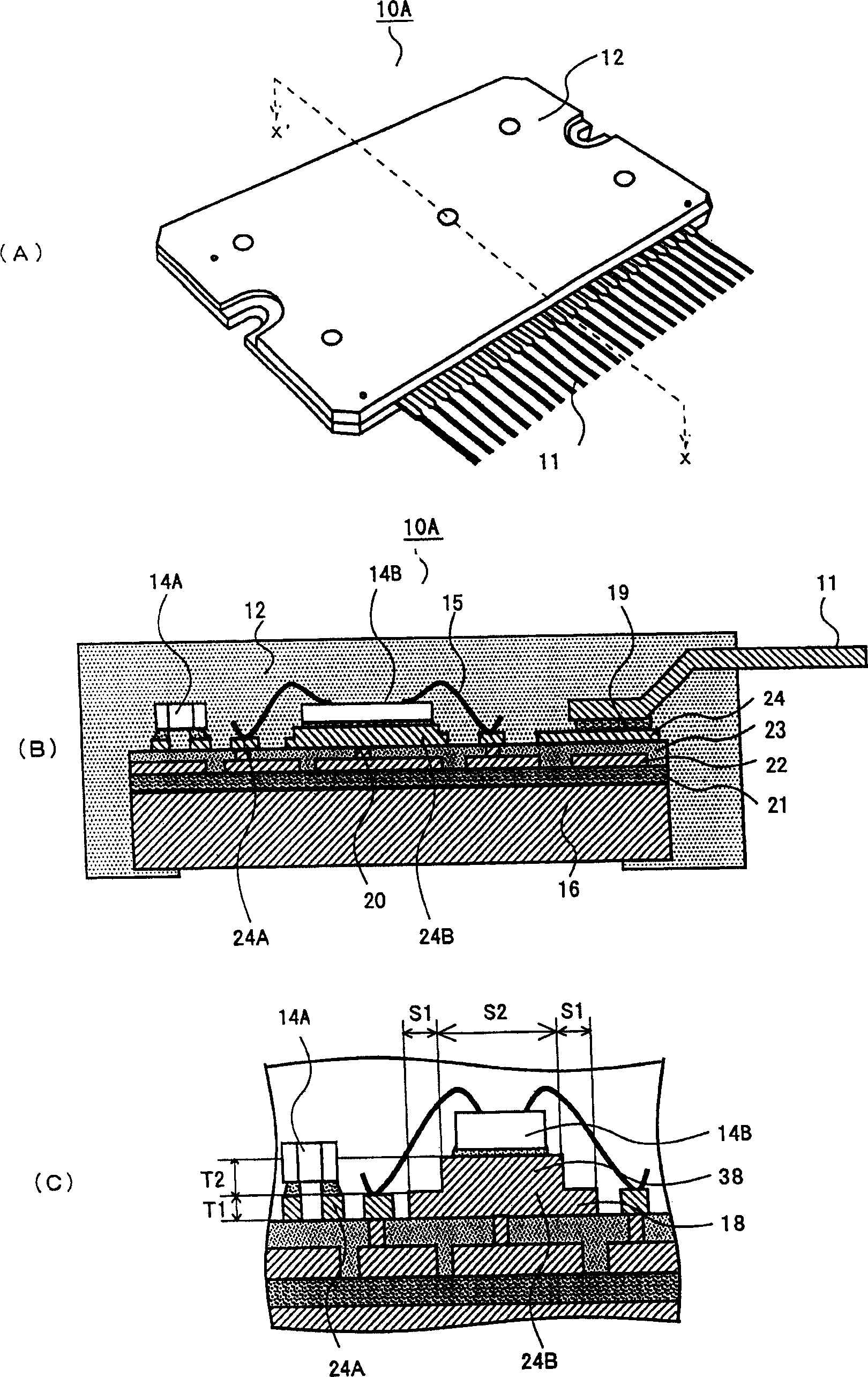
[0043] refer to figure 1 The configuration of the circuit device 10A of this embodiment will be described. figure 1 (A) is a perspective view of the circuit device 10A, figure 1 (B) is figure 1 (A) Cross-sectional view of X-X' section. figure 1 (C) is a cross-sectional view showing the portion of the second pattern 24B of this embodiment.

[0044] In this embodiment, the first insulating layer 21 is formed on the surface of the circuit board 16 made of aluminum, and the first wiring layer 22 is formed on the surface of the first insulating layer 21 . In addition, the second insulating layer 23 is formed on the surface of the first wiring layer 22, and the second wiring layer 24 is formed on the surface of the second insulating layer 23 to constitute a multilayer structure. In addition, the second wiring layer 24 is composed of a first conductive pattern 24A and a second conductive pattern 24B formed thicker than the first conductive pattern 24A. Furthermore, the back...

no. 2 example

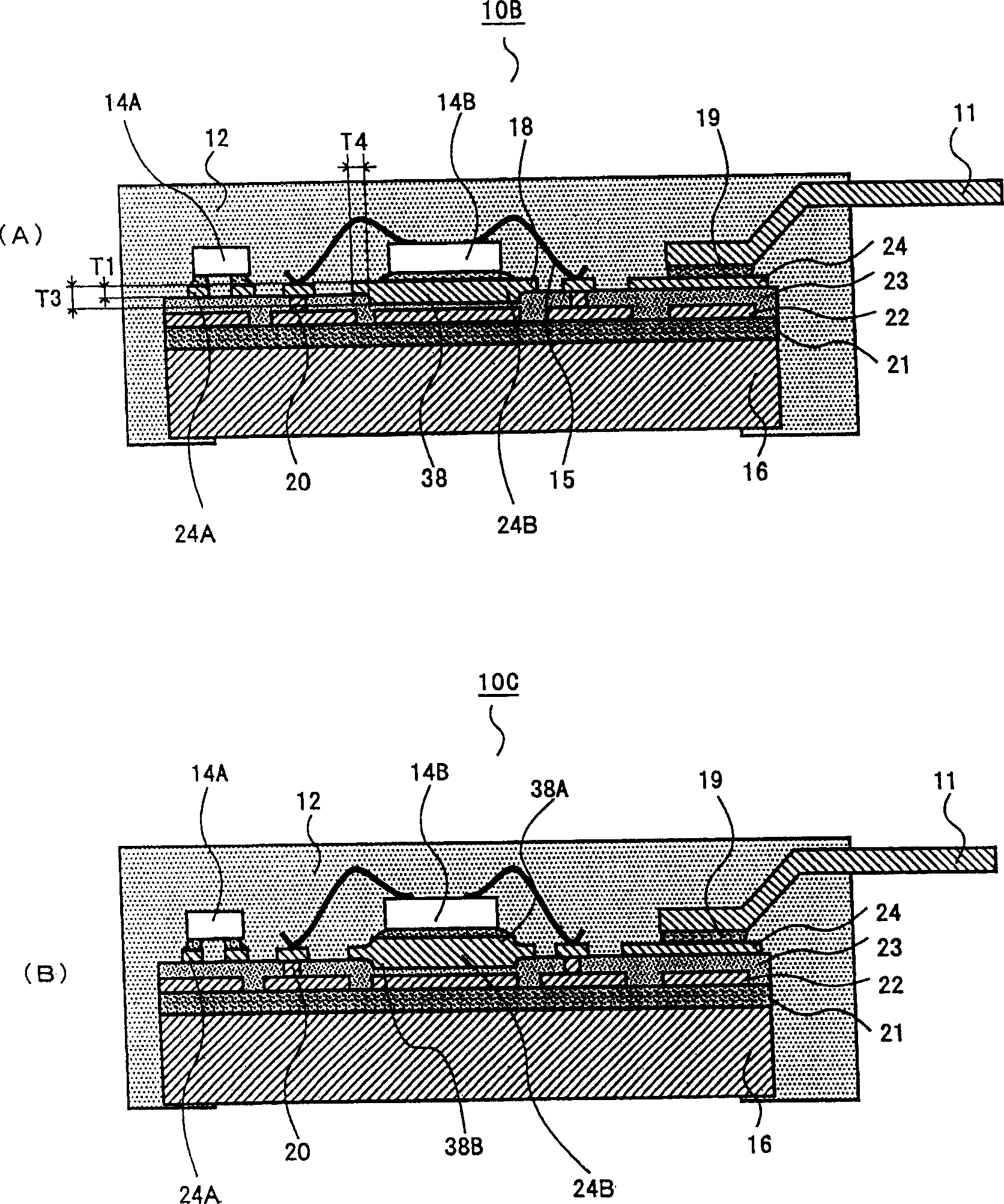
[0121] refer to Figure 13 The circuit device 40 of this embodiment will be described. Figure 13 Each of the drawings is a cross-sectional view of the circuit device of this embodiment.

[0122] refer to Figure 13 (A), a multilayer wiring structure composed of two wiring layers is formed on the circuit device 40A. The upper first wiring layer 41 is composed of a first conductive pattern 41A and a second conductive pattern 41B formed thicker than the first conductive pattern 41A. Furthermore, the back surfaces of the first conductive pattern 41A and the second conductive pattern 41B are arranged substantially at the same level, and the convex portion 38 is formed so that the surface of the second conductive pattern 41B is located above the surface of the first conductive pattern 41A. First, let the thickness of the first conductive pattern 41A be T1, and let the thickness of the second conductive pattern 41B be T3. In order to finely form the first conductive pattern 41A,...


PUM


Abstract

A circuit device which enables formation of a minute pattern while securing a current capacity and has excellent heat release properties, and a manufacturing method thereof are provided. In a circuit device of the present invention, among multiple wiring layers, a first wiring layer is formed of a thin first conductive pattern and a thick second conductive pattern. Therefore, formation of the minute patterns is realized while securing the current capacity. Moreover, a small-signal circuit element is mounted on the first conductive pattern, and a large-current circuit element is mounted on the second conductive pattern. Thus, circuit elements having different sizes of currents to be handled are mounted on the same board. Furthermore, heat release properties are improved by the second conductive pattern which is formed to be thick.

Description

technical field [0001] The present invention relates to a circuit device and its manufacturing method, in particular to a circuit device having a multilayer wiring structure with conductive patterns having different thicknesses and its manufacturing method. Background technique [0002] First, refer to Figure 22 The configuration of a conventional hybrid integrated circuit will be described (for example, refer to Patent Document 1). Figure 22 (A) is a perspective view of the hybrid integrated circuit device 100, Figure 22 (B) is Figure 21 (A) X-X' line profile. [0003] The existing hybrid integrated circuit device 100 has the following structure, which includes: a rectangular substrate 106; an insulating layer 107, which is arranged on the surface of the substrate 106; a conductive pattern 108, which is formed on the insulating layer 107; circuit elements 104, which are fixed On the conductive pattern 108; thin metal wire 105, which electrically connects the circuit el...

Claims


Application Information

Patent Timeline
Patent Type & Authority Applications(China)
IPC IPC(8): H01L23/29H01L23/12H01L23/538H01L25/04H01L25/18H05K1/02H05K1/05H05K3/28H05K3/46H05K7/06
CPCH05K1/0203H01L2924/19105H01L2924/01046H05K3/4647H05K3/284H01L2924/01025H01L2224/32245H05K2203/049H01L2924/01019H01L2924/15311H05K1/0265H05K1/0206H01L2924/19041H01L2224/48472H01L2224/48091H01L23/538H01L2924/30107H01L2224/32225H05K3/4652H05K2203/1476H01L23/5383H01L24/48H01L2924/01079H01L2224/48465H05K2201/0355H01L2224/48227H05K2201/09736H05K1/056H05K2201/10969H01L2924/0102H01L2924/01078H01L2924/10253H01L2924/01012H05K2203/1189H01L2224/73265H05K2203/0369H01L2924/13055H01L24/45H01L24/49H01L24/73H01L2224/45015H01L2224/451H01L2224/4903H01L2924/00014H01L2924/07802H01L2924/12042H01L2924/1301H01L2924/13034H01L2924/14H01L2924/181Y10T29/49155H01L2924/00H01L2924/00012H01L2924/00015H01L2924/20758H01L2224/05599H01L23/48
Inventor 五十岚优助高草木贞道
Owner SANYO ELECTRIC CO LTD
Why Eureka
Try Eureka