Thin film transistor array panel and display device including the same

A technology of thin film transistors and array panels, which is applied in the field of display devices and can solve problems such as sealant hardening and gate drive circuit corrosion

Active Publication Date: 2006-02-01
SAMSUNG DISPLAY CO LTD
View PDF2 Cites 34 Cited by
  • Summary
  • Abstract
  • Description
  • Claims
  • Application Information

AI Technical Summary

Problems solved by technology

However, irradiation from the TFT array panel side may result in insufficient light to harden the encapsulant, especially when the width of the signal lines or transistors in the gate drive circuit is greater than 100 μm
As a result, the two panels may be susceptible to moisture ingress through the insufficiently hardened encapsulant, causing corrosion of the gate drive circuitry

Method used


Image

  • Thin film transistor array panel and display device including the same
  • Thin film transistor array panel and display device including the same
  • Thin film transistor array panel and display device including the same

Examples


Embodiment Construction

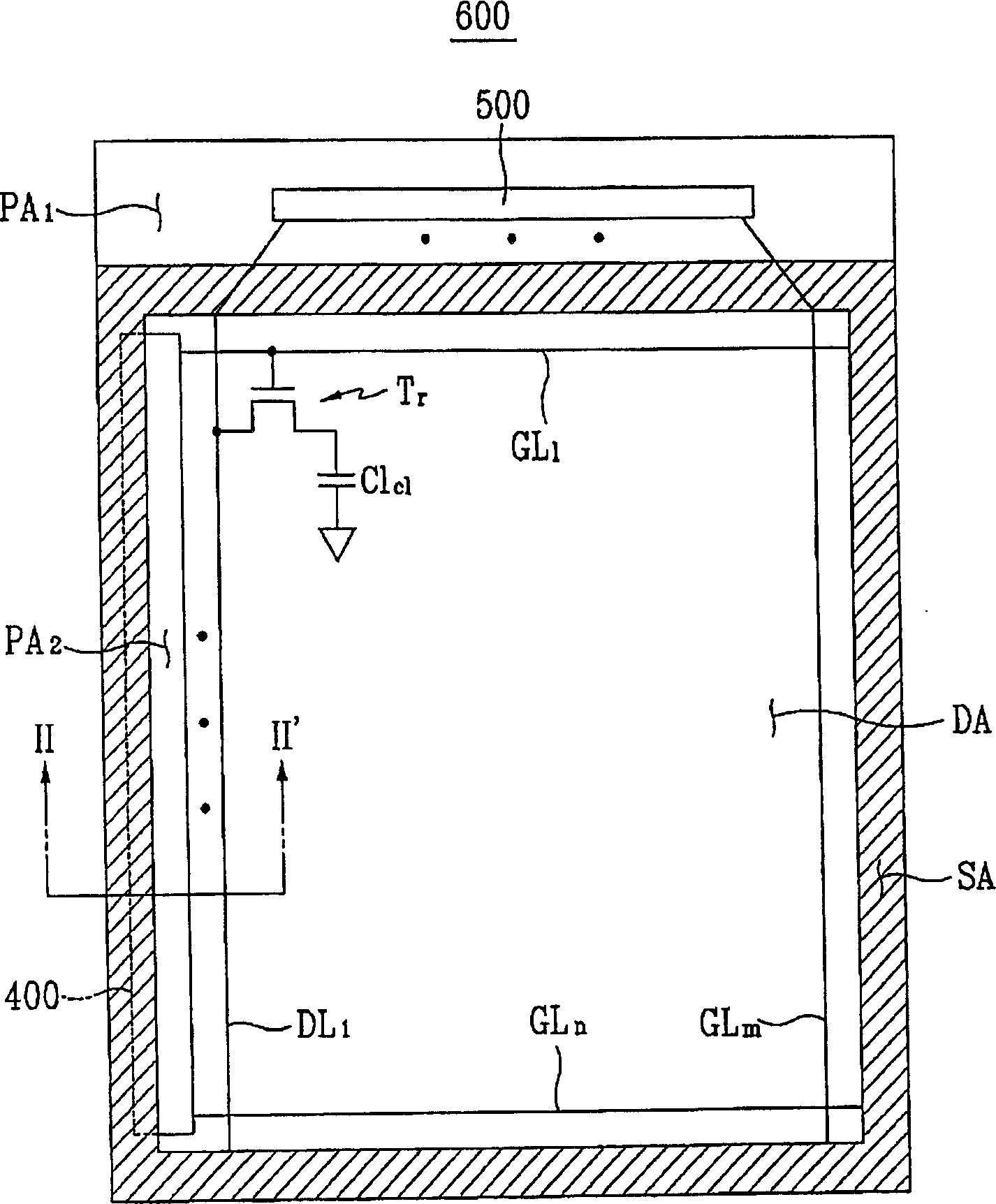
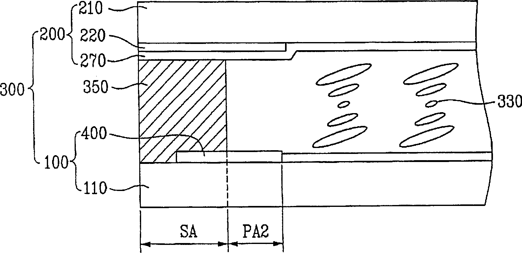
[0023] figure 1 is an example layout diagram of a display device 600 according to an embodiment of the present invention, and figure 2 is along figure 1 Sectional view of line II-II'. Such as figure 1 with 2 As shown, the display device 600 includes a display panel 300 for displaying images under the control of the gate signal and the data signal respectively provided by the gate drive circuit 400 and the data drive circuit 500 . The display area DA and the gate driving circuit 400 can be formed on a single substrate, such as figure 2 on the substrate 110.

[0024] The display panel 300 includes a thin film transistor array panel 100; an opposite panel 200 facing the thin film transistor array panel 100; a sealant 350 and a liquid crystal provided in a space surrounded by the thin film transistor array panel 100, the opposite panel 200, and the sealant 350 Layer 330.

[0025] The display panel 300 can be divided into a display area DA, a sealing area SA surrounding th...


PUM

PropertyMeasurementUnit
widthaaaaaaaaaa
widthaaaaaaaaaa

Abstract

Gate-driving circuitry of a thin film transistor array panel is formed on the same plane as a display area of the transistor array panel. The gate-driving circuitry includes driving circuitry and signal lines having apertures. Thus, a sufficient amount of light, even though illuminated from the thin film transistor array panel side, can reach a photosetting sealant overlapping at least in part the gate-driving circuitry. The thin film transistor array panel and the counter panel are put together air-tight and moisture-tight. Consequently, the gate-driving circuitry can avoid corrosion by moisture introduced from outside. Gate-driving circuitry malfunctions can also be reduced.

Description

technical field [0001] The present invention relates to display device technology, and more particularly, relates to the design and application of a thin film transistor array panel and a display device including such a thin film transistor array panel. Background technique [0002] Generally, a display device includes a display panel, a gate driving circuit and a data driving circuit. The display panel includes a thin film transistor array panel having gate lines, data lines, pixel electrodes, and thin film transistors; an opposite panel having one or more common electrodes; and a liquid crystal layer provided between the two panels. The two panels are aligned and sealed with sealant. The gate driving circuit and data driving circuit are usually provided on a printed circuit board, or as an integrated circuit connected to the display panel. [0003] Recently, in order to minimize device size and increase efficiency, gate driving circuits have been directly formed on thin ...

Claims


Application Information

Patent Timeline
Patent Type & Authority Applications(China)
IPC IPC(8): G02F1/136G02F1/133G09G3/36G09F9/35
CPCG02F1/136286G02F1/1368G09G3/3648G09G3/3696
Inventor 金东奎文胜焕李龙淳姜南洙朴倖源
Owner SAMSUNG DISPLAY CO LTD
Why Eureka
Try Eureka