Semiconductor device and method for manufacturing the same

A technology of semiconductor and opening position, applied in the direction of semiconductor devices, electric solid devices, electrical components, etc., can solve the problems of energy loss, quality factor value reduction, etc., and achieve the effect of reduced energy loss, high Q value, and reduced loss

Inactive Publication Date: 2006-02-01
THE FUJIKURA CABLE WORKS LTD
View PDF3 Cites 2 Cited by
  • Summary
  • Abstract
  • Description
  • Claims
  • Application Information

AI Technical Summary

Problems solved by technology

[0023] (1) Because the lower wiring layer 21 is close to the semiconductor substrate 1, C Si energy loss due to increased parasitic capacitance
[0024] (2) Since the lower wiring layer 21 and the upper wiring layer 23 (helical coil 24) are close, C S increase, resulting in energy loss
[0026] (1) Because the lower wiring layer 24 is close to the semiconductor substrate 1, R Si Increased due to eddy current losses resulting in energy loss
[0027] (2) Since the lower wiring layer 21 and the upper wiring layer 23 (helical coil 24) are close, C S increase, resulting in energy loss
[0029] However, in conventional semiconductor devices, multilayer wiring structures may be required
In this case, impedance mismatch occurs at junctions (contact holes) connecting wires and inductive elements formed in different layers, which can lead to a decrease in quality factor value (Q value)

Method used


Image

  • Semiconductor device and method for manufacturing the same
  • Semiconductor device and method for manufacturing the same
  • Semiconductor device and method for manufacturing the same

Examples


example

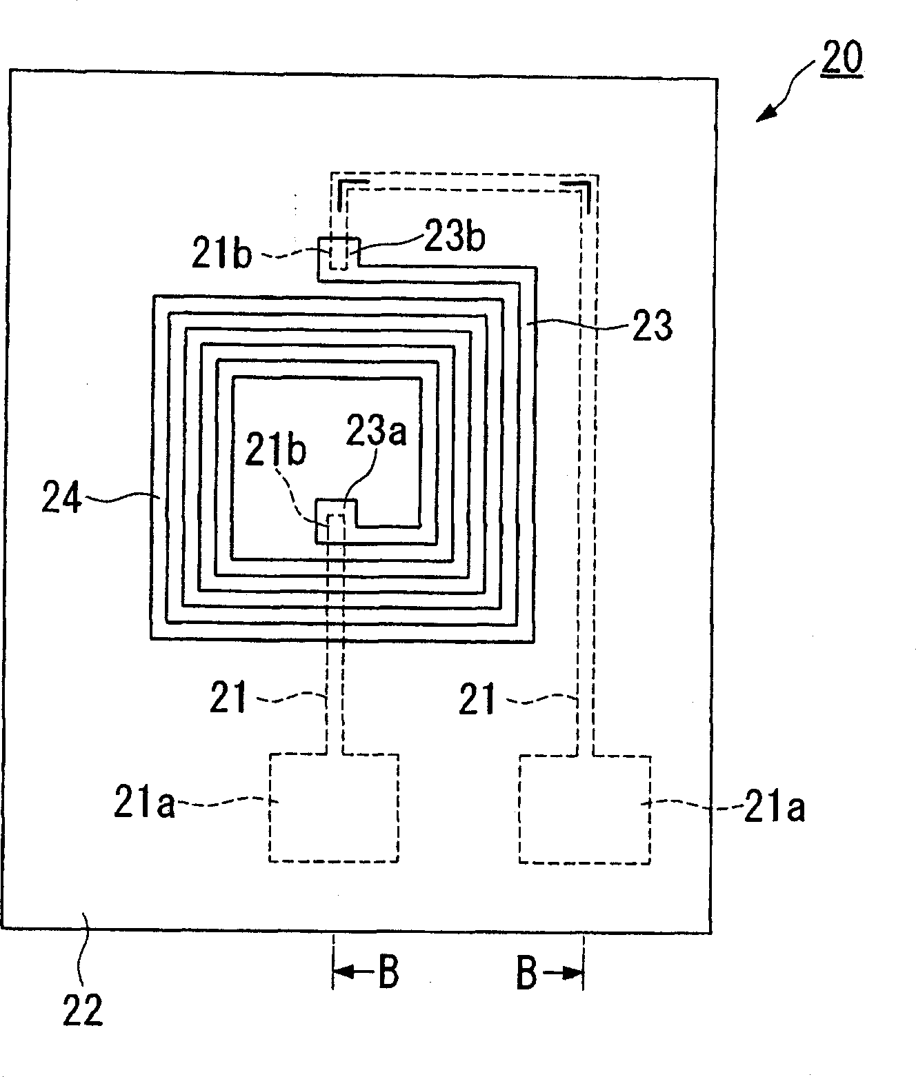
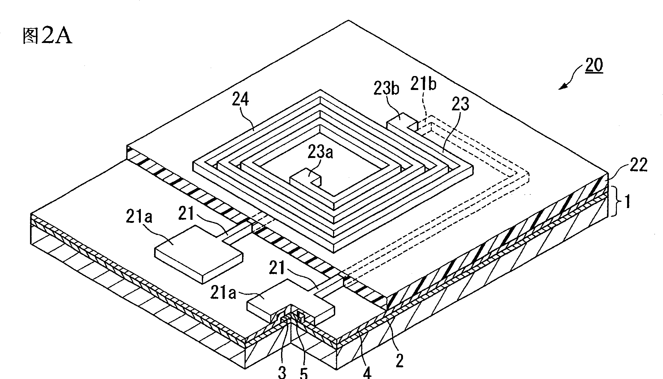
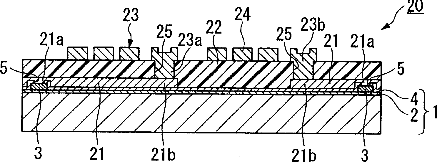
[0113] Manufacture of semiconductor devices and evaluation of their characteristics. A silicon substrate is used as the semiconductor substrate. The first insulating resin layer and the second insulating resin layer are formed of polyimide resin. A first wiring layer is provided between the first insulating resin layer and the second insulating resin layer, and a second wiring layer is provided on the second insulating resin layer. The dielectric element was formed as a 3.5-turn helical coil. Copper (Cu) is used as the material of the first wiring layer and the second wiring layer.

[0114] Location of the sensing element

[0115] As a working example of the present invention, a semiconductor device having a first wiring layer near the semiconductor substrate as an interconnection (lower path) and a second wiring layer away from the semiconductor substrate as a dielectric element was fabricated . As a comparative example, a semiconductor device having a first wiring layer...


PUM


Abstract

A semiconductor device includes a semiconductor substrate having an electrode formed above a surface thereof; a first insulating resin layer that is provided over the semiconductor substrate and has a first opening defined at a position corresponding to the electrode; a first wiring layer that is provided on the first insulating resin layer and is connected to the electrode through the first opening; a second insulating resin layer provided over the first insulating resin layer and the first wiring layer, the second insulating resin layer having a second opening that is defined at a position different from the position of the first opening in a direction of the surface of the semiconductor substrate; and a second wiring layer that is provided on the second insulating resin layer and is connected to the first wiring layer through the second opening, wherein the second wiring layer includes an induction element, and a sum of a thickness of the first insulating resin layer and a thickness of the second insulating resin layer is not less than 5 mum and not more than 60 mum.

Description

technical field [0001] The present invention relates to a semiconductor device and a method of manufacturing the same, wherein the formation of a semiconductor having an inductive element formed on a semiconductor substrate such as a silicon wafer is accomplished together with its packaging. [0002] Priority is claimed on Japanese Patent Application No. 2004-221785 filed on July 29, 2004 and Japanese Patent Application No. 2004-302696 filed on October 18, 2004, the contents of which are incorporated herein by reference. Background technique [0003] In recent years, in the manufacture of high-frequency semiconductor elements, in order to ensure impedance matching and the like, inductive elements, such as spiral inductors, are formed on semiconductor substrates. In such a semiconductor element, however, due to parasitic capacitance between the wiring and the semiconductor substrate, part of the electromagnetic energy generated by the inductive element is lost in the substrat...

Claims


Application Information

Patent Timeline
Patent Type & Authority Applications(China)
IPC IPC(8): H01L27/04
Inventor 糸井和久佐藤正和伊藤达也
Owner THE FUJIKURA CABLE WORKS LTD
Why Eureka
Try Eureka