Opposite target reaction magnetocontrol sputtering method for preparing vanadium oxide film
A reactive magnetron sputtering, vanadium oxide thin film technology, applied in sputtering coating, ion implantation coating, metal material coating process, etc., can solve the problem of low target material utilization, elevated substrate temperature, high temperature and other problems, to achieve the effect of high target utilization rate, low substrate temperature and high sputtering rate
- Summary
- Abstract
- Description
- Claims
- Application Information
AI Technical Summary
Problems solved by technology
Method used
Image
Examples
Embodiment 1
[0016] Embodiment 1 prepares the vanadium oxide film of high temperature coefficient of resistance on a glass substrate, and concrete steps are as follows:
[0017] 1) Cleaning the glass substrate, the process is as follows: ultrasonically clean with acetone, rinse with deionized water, then ultrasonically clean with ethanol, and then rinse with deionized water;
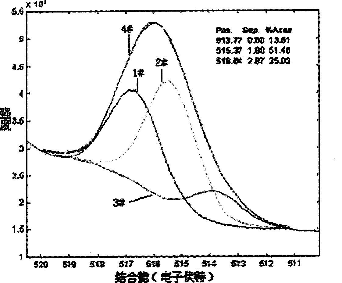
[0018] 2) Prepare a vanadium oxide thin film on the above glass substrate by using the reactive magnetron sputtering method against the target, open the vacuum chamber, put the glass substrate, first draw a low vacuum, then open the high valve, and draw a high vacuum to 3×10 -4 Below Pa, flow argon and oxygen with a flow volume ratio of 120:1 into the vacuum chamber to a working pressure of 2Pa, and sputter the film with a sputtering power of 240W, a substrate temperature of 25°C, and a sputtering time of 30 minutes. . ;
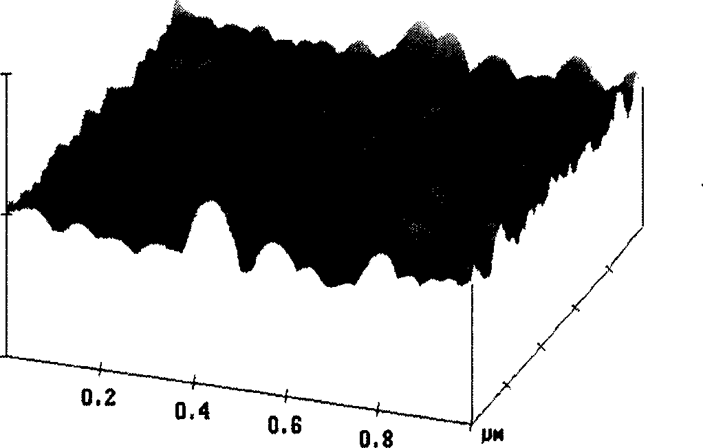
[0019] 3) The above-mentioned vanadium oxide film was tested for resistance temperature chara...
Embodiment 2
[0020] Embodiment 2 prepares the vanadium oxide thin film of high temperature coefficient of resistance on silicon substrate, concrete steps are as follows:
[0021] 1) The surface of the silicon wafer is cleaned to remove polluting organic matter, dust and metal ion impurities on the surface of the silicon wafer. The process is as follows: concentrated sulfuric acid (concentration is 98%) and hydrogen peroxide are mixed in a volume ratio of 3:1 to prepare a cleaning solution. Soak the silicon chip in this cleaning solution for 40 minutes, rinse the silicon chip with deionized water, then mix ammonia water, hydrogen peroxide and deionized water in a volume ratio of 1:40:50, soak the silicon chip for 30 minutes, and then wash it with deionized water rinse. A layer of silicon oxide film was first deposited on the silicon wafer by PECVD method, and the back vacuum was 4.5×10 -1 Pa, working pressure is 4.3Pa, substrate temperature is 150℃, working gas is N 2 O and SiH 4 , the g...
Embodiment 3
[0025] This embodiment is similar to embodiment 2, except that the process parameters of step 2 are: the argon gas and oxygen gas with a flow volume ratio of 130:1 are passed into the vacuum chamber to a working pressure of 1.5Pa, the sputtering power is 195W, and the sputtering power is 195W. The irradiation time was 75 minutes, the substrate temperature was 200°C, and the resistance-temperature characteristic test was carried out on the vanadium oxide thin film. -2 K -1 .
PUM
| Property | Measurement | Unit |
|---|---|---|
| Temperature coefficient of resistance | aaaaa | aaaaa |
| Temperature coefficient of resistance | aaaaa | aaaaa |
Abstract
Description
Claims
Application Information


