Automatic testing device of semiconductor construction element

An automated testing and semiconductor technology, applied in the direction of single semiconductor device testing, etc., can solve problems such as the inability to fully expose system-level interactions in semiconductor chips, reduce testing costs and testing time, simplify testing procedures, and improve error coverage. Effect

Active Publication Date: 2006-03-29
CHROMA ATE
View PDF0 Cites 9 Cited by
  • Summary
  • Abstract
  • Description
  • Claims
  • Application Information

AI Technical Summary

Problems solved by technology

That is to say, after the complete semiconductor final test process, the system-level interaction proble

Method used


Image

  • Automatic testing device of semiconductor construction element
  • Automatic testing device of semiconductor construction element
  • Automatic testing device of semiconductor construction element

Examples


Embodiment Construction

[0017] The aforementioned and other technical contents, features and effects of the present invention will be clearly understood in the following detailed description of preferred embodiments with reference to the accompanying drawings.

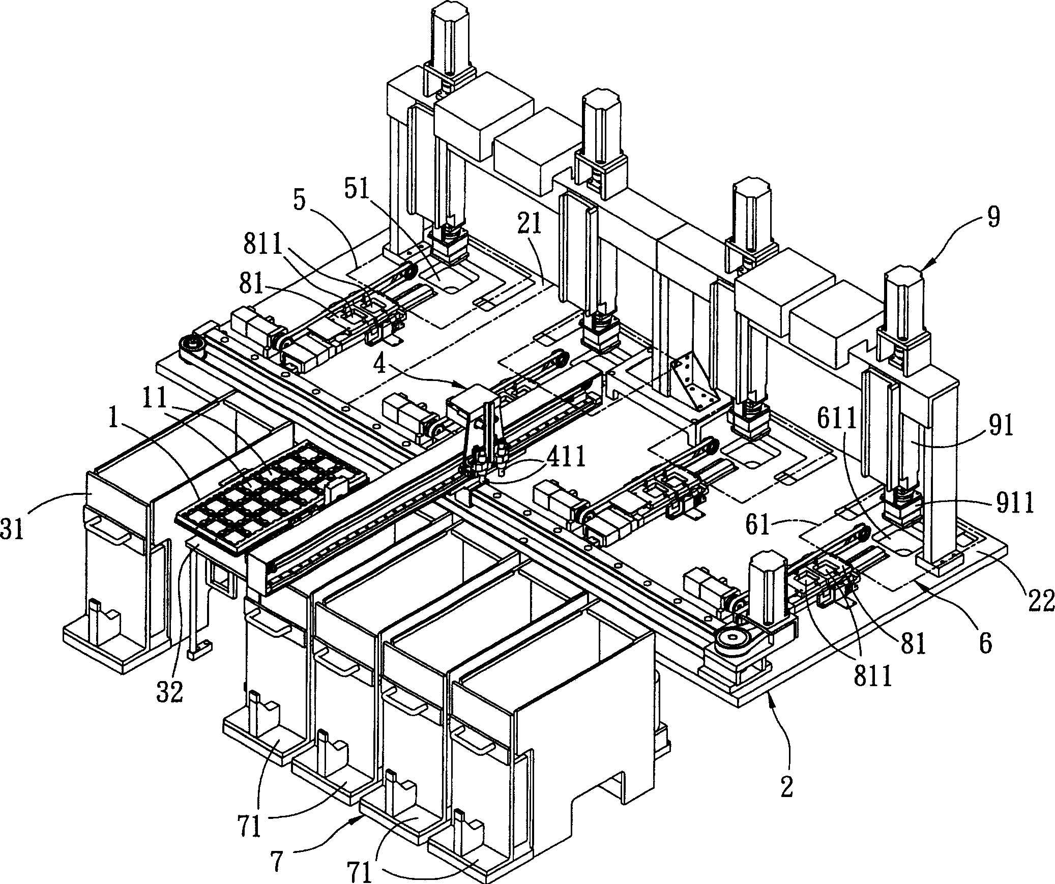
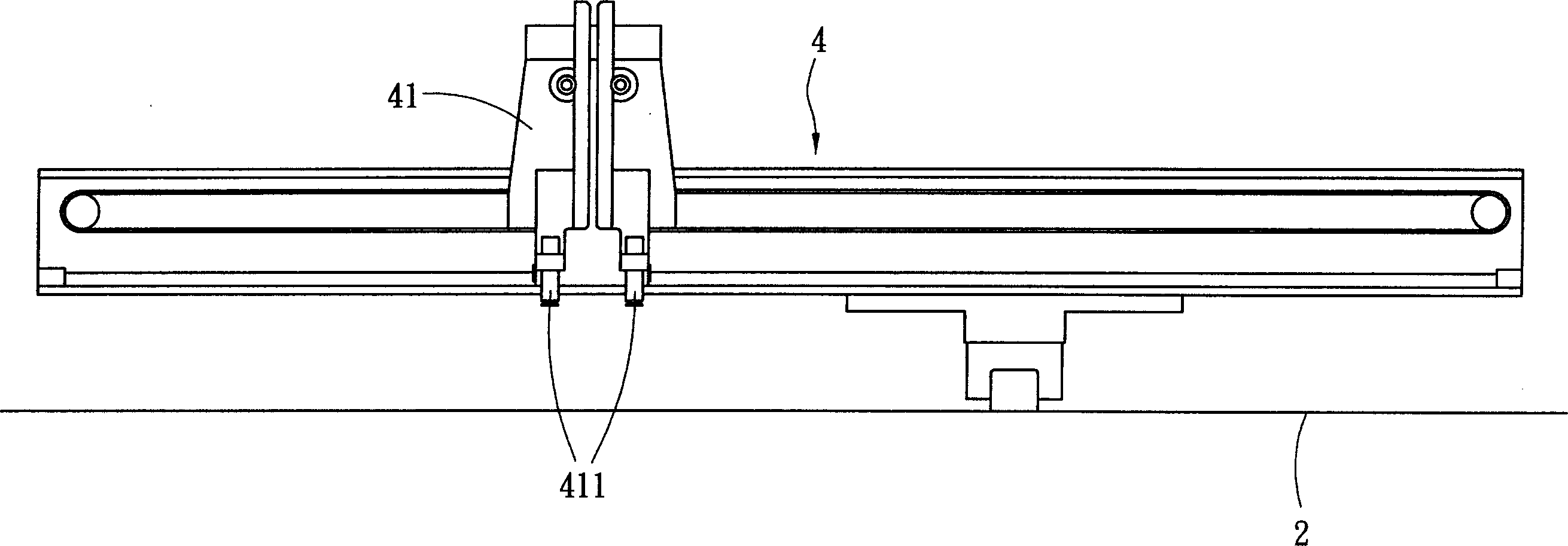
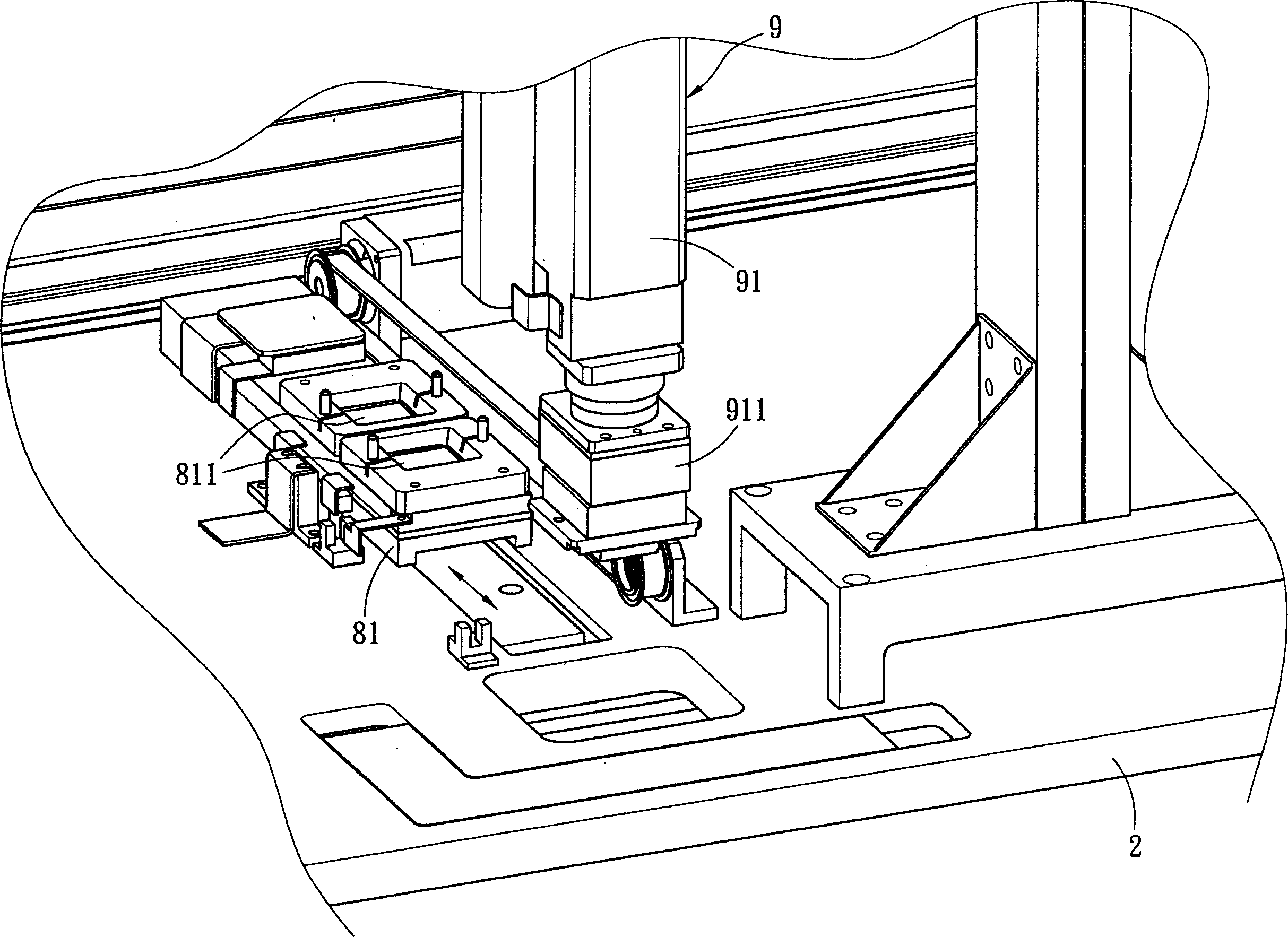
[0018] see figure 1 , 2 Shown, according to the automatic testing device of semiconductor package element of the present invention, be suitable for the semiconductor testing process after packaging, the preferred embodiment of the automatic testing device of this semiconductor package component comprises: a working platform 2, a feeding unit 3. A conveying unit 4 , a first testing unit 5 , a second testing unit 6 , and a discharging unit 7 .

[0019] The working platform 2 has a first test area 21 with a smaller area and a second test area 22 with a larger area. The feeding unit 3 is disposed on the front end of the working platform 2 and adjacent to the working platform 2 , and has a feeding box 31 . A plurality of semiconductor carrier p...


PUM


Abstract

The present invention discloses automatic testing equipment for semiconductor element. Said equipment includes the following several portions: a working platform, a feeding unit, a conveying unit, a first testing unit, a second testing unit and a discharge unit. Said invention also provides the concrete action of every portion, and provides connection mode of the above-mentioned all the portions.

Description

technical field [0001] The invention relates to a test device, in particular to an automatic classification test device for semiconductor assembly components. Background technique [0002] The final test process of the semiconductor is to test the performance of the assembled product through a test equipment (TESTER) after the semiconductor element is assembled, so as to ensure the functional integrity of the semiconductor assembled element in the factory, and to test the The products are classified and screened according to their performance as the evaluation basis for different grades of semiconductor components. [0003] However, with the rapid development of technology, the functions of many semiconductor chips are becoming more and more diversified, and the operating speed is also increasing. The functions of the existing testing equipment are gradually no longer able to meet the test of the semiconductor chip. Even if the manufacturer releases the corresponding testin...

Claims


Application Information

Patent Timeline
IPC IPC(8): G01R31/26
Inventor 欧阳勤一
Owner CHROMA ATE
Why Eureka
Try Eureka