

Pattern checking device
An inspection device and pattern technology, applied in measurement devices, optical devices, material analysis by optical means, etc., can solve the problems of difficult inspection, narrow space between wirings, etc., and achieve the effect of reducing reflected light components and excellent contrast.
- Summary
- Abstract
- Description
- Claims
- Application Information
AI Technical Summary
Problems solved by technology
Method used
Image

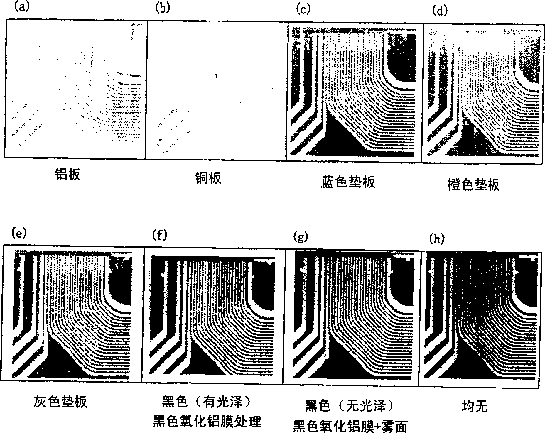
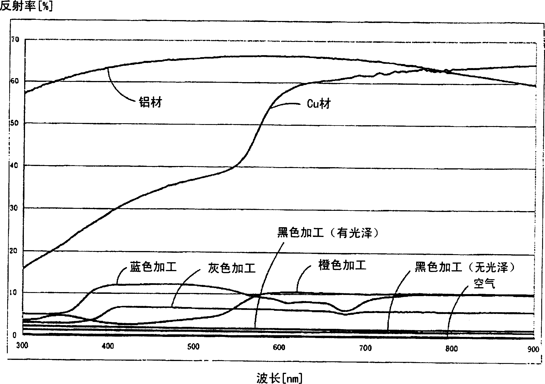
Examples
Embodiment Construction
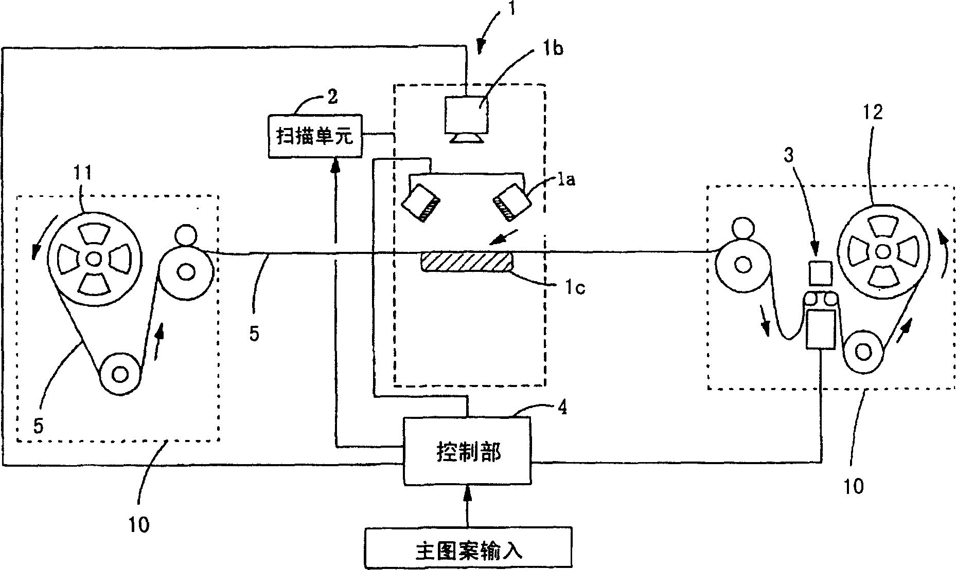
[0069] figure 1 It is a block diagram showing a schematic configuration of the wiring pattern inspection device according to the first embodiment of the present invention. In addition, although the wiring pattern inspection of the TAB tape is described in the following examples, the present invention can also be applied to the case of inspecting the pattern formed on the polyimide resin film using reflected illumination light other than the TAB tape.
[0070] The pattern inspection device of this embodiment includes a tape conveying mechanism 10 ;
[0071] In the vicinity of the winding coiler 12, a marking unit 3 for marking a defective pattern is provided. In the marking part 3, the pattern judged to be unacceptable is punched with a puncher, or marking such as coloring is carried out so that the part can be immediately confirmed as unacceptable by visual inspection.
[0072] The TAB tape 5 fed out from the feeding winder 11 is sent to the inspection unit 1 . Conveyance ...
PUM
 Abstract
Description
Claims
Application Information