

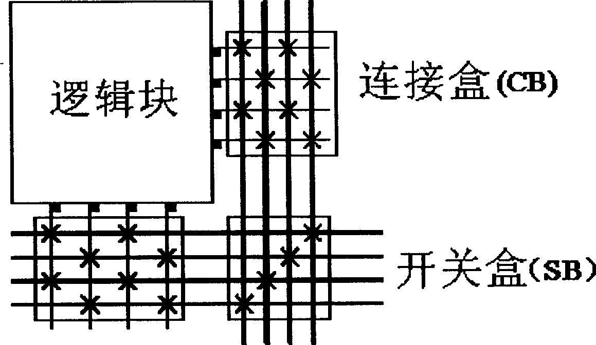
General in-situ programmeable gate array configuration wiring model
A layout and routing, gate array technology, applied in the field of VLSI, can solve problems such as complex structure of FPGA
- Summary
- Abstract
- Description
- Claims
- Application Information
AI Technical Summary
Problems solved by technology
Method used
Image

Examples
Embodiment Construction
[0051] In order to illustrate the method used herein, the technical solutions and implementation steps herein are described in detail for specific examples.
[0052] (I) Improvement of the connection box CB
[0053] In this model, the flexibility of CB is extended to specify the connection between any pin and the routing resources in the channel, so that the VPR model is no longer limited to the singleness of the pin connection.
[0054] Take the alu4 test circuit in Table 1 as an example, the specific method is as follows:
[0055] For the pins of the model of the present invention, there are the following connections:
[0056] β(P 1 )=(1, TOP, 1, 1, 0, 1, 1, 1, 0, 1, 1, 0) the first pin, the position is on the top, and the pin is connected with the third, seventh, and tenth horizontal wiring resources no connection
[0057] β(P 2 )=(2, BOTTOM, 1, 0, 1, 0, 1, 0, 1, 0, 1, 1) the second pin, the position is below, and the pin is the second, fourth, sixth, eighth Routing r...
PUM
 Abstract
Description
Claims
Application Information