

System and method for identifying changing of workpiece parameter
A technology for parameter changes and workpieces, applied in electrical components, manufacturing tools, metal processing equipment, etc., to solve problems such as missing end points, weak signals, and ambiguity
- Summary
- Abstract
- Description
- Claims
- Application Information
AI Technical Summary
Problems solved by technology
Method used
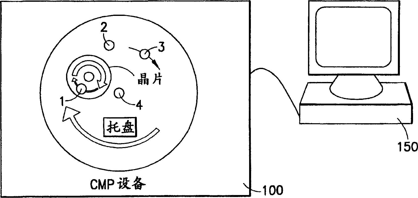
Image

Examples
Embodiment Construction
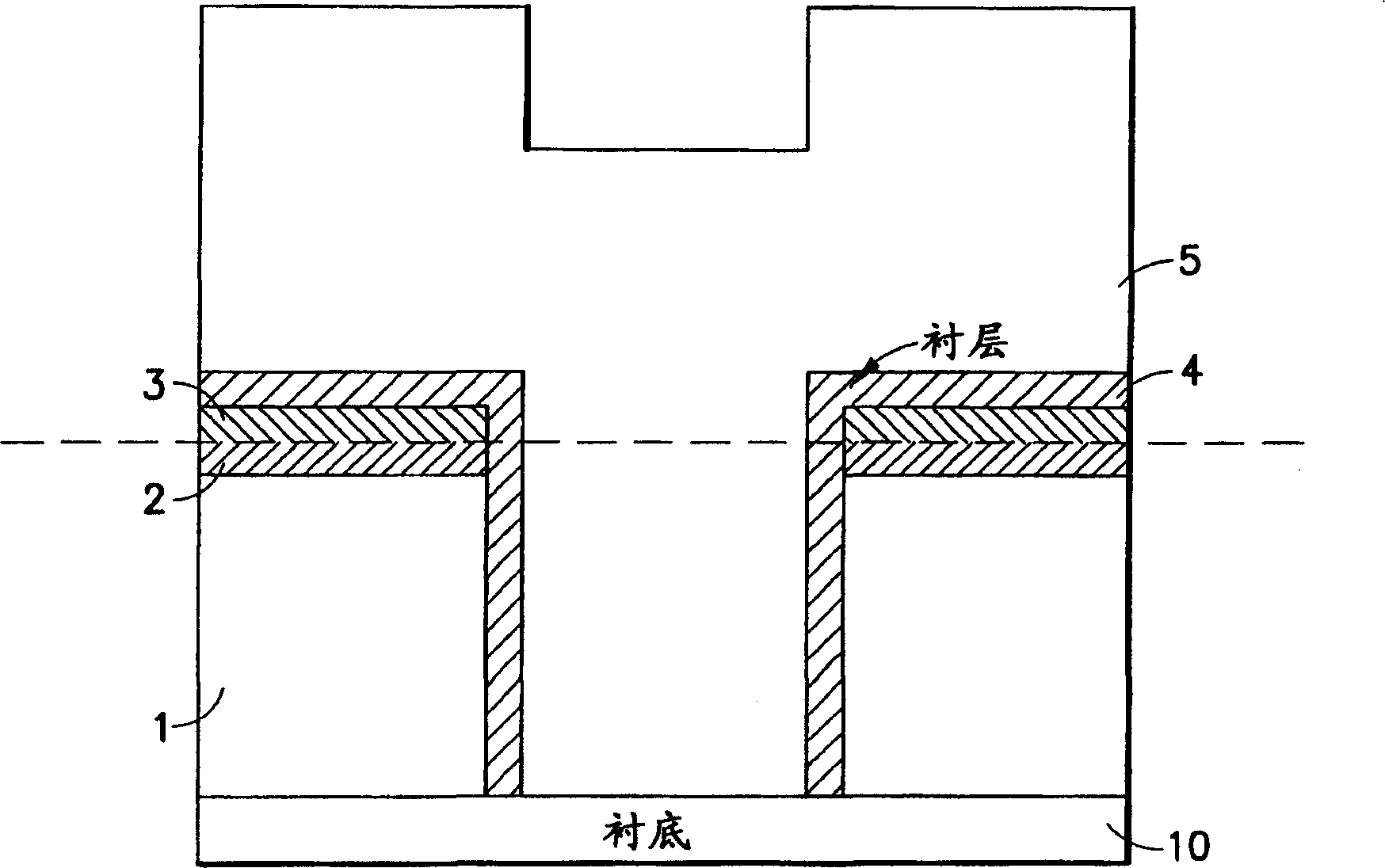
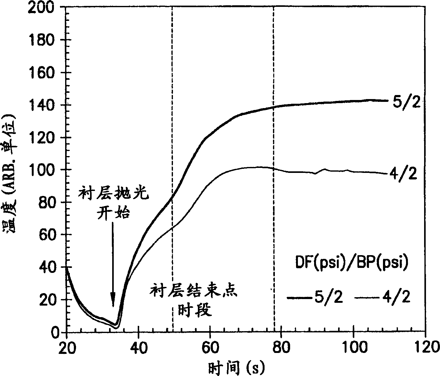
[0021] See figure 1 , the semiconductor structure has a first dielectric layer 1 and hard mask / CMP polish stop layers 2 and 3 . The interface between layer 3 and layer 2 is the interface to be detected or set as a stop point. Depending on the application, the fill material can be metal or dielectric.
[0022] The present invention is directed to the detection of CMP end points when polishing layers of chemically similar material, for example comprising a first dielectric of single damascene or dual damascene thickness (or multiple layers comprising embedded etch stop layers dielectric stack), and a multilayer spin-on or plasma-enhanced chemically vapor deposited (PECVD) CMP stop layer (or "capping layer") on the first dielectric layer "(cap layer)). The first dielectric layer may consist of the following substances: SiLK TM , GX-3 TM , Porous SiLK (TM) , GX - threesome (TM) , Black Diamond TM , NCS TM or other non-porous or porous low-k dielectric materials. The CMP...
PUM
 Abstract
Description
Claims
Application Information