
Encapsulation structure for multiple chips

A multi-chip packaging and chip technology, applied in electrical components, electrical solid devices, circuits, etc., can solve the mismatch of thermal expansion coefficient of packaging structure, affect the reliability of packaging structure, increase the overall thickness of packaging structure, packaging process and material cost, etc. question

Inactive Publication Date: 2006-07-05
MACRONIX INT CO LTD
View PDF0 Cites 1 Cited by
  • Summary
  • Abstract
  • Description
  • Claims
  • Application Information

AI Technical Summary

Problems solved by technology

As a result, it is bound to increase the overall thickness of the packaging structure, packaging process and material costs
At the same time, since the packaging structure has materials with different coefficients of thermal expansion (CTE), such as chip holders, dummy chips or spacers, chips, inner leads, and encapsulants, the packaging structure will have serious thermal expansion coefficients. Matching problems, which in turn affect the reliability of the package structure

Method used


Image

  • Encapsulation structure for multiple chips
  • Encapsulation structure for multiple chips
  • Encapsulation structure for multiple chips

Examples


Embodiment 1

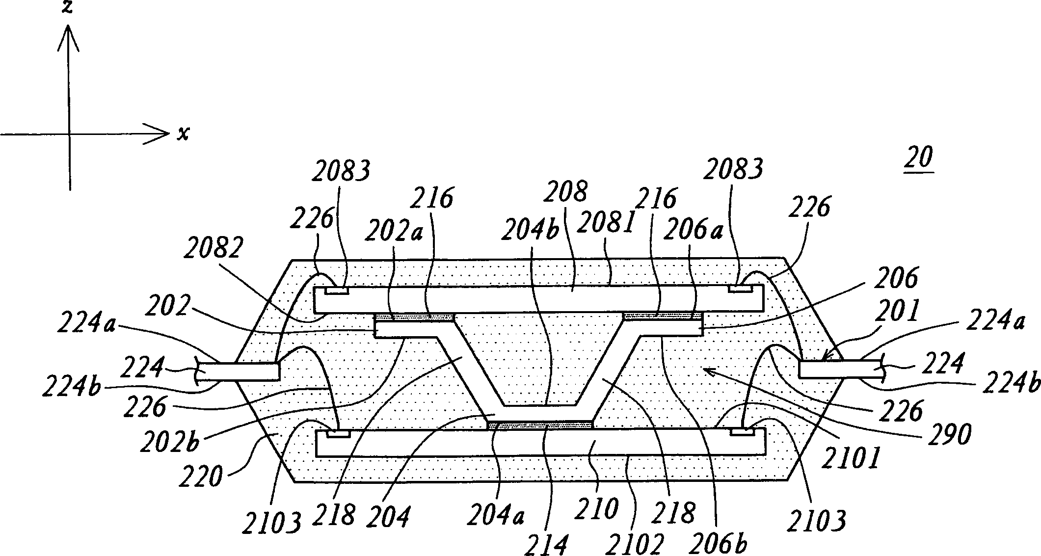
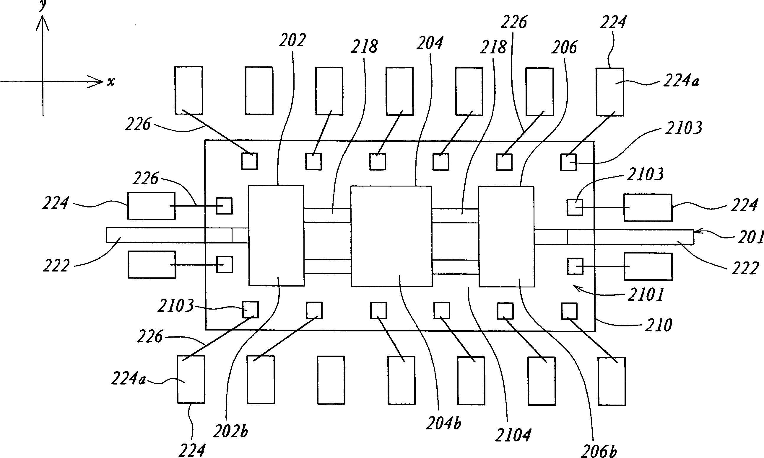
[0045] Please refer to figure 2 , which shows a cross-sectional view of the multi-chip packaging structure according to Embodiment 1 of the present invention. exist figure 2 Among them, the multi-chip package structure 20 includes a lead frame 201 , two chips 208 and 210 with the same or similar size, several wires 226 and an encapsulant 220 . In order to allow the active surfaces of chips 208 and 210 with similar or identical dimensions to face the same direction, the lead frame 201 is specially designed in this embodiment. The chip pad connection structure 218 connecting the first chip pad and the second chip pad and several inner pins 224 surrounding the periphery of the first chip pad and the second chip pad.

[0046] The first chip mount has a first die-bonding surface and a first non-die-bonding face opposite to each other, the second die mount has a second die-bonding face and a second non-die-bonding face opposite, and the die mount connection structure 218 is conn...

Embodiment 2

[0052] Please refer to Figure 4 , which shows a cross-sectional view of the multi-chip packaging structure according to Embodiment 2 of the present invention. The difference between the multi-chip packaging structure 20a of this embodiment and the multi-chip packaging structure 20 of Embodiment 1 is that the multi-chip packaging structure 20a of this embodiment further includes a chip 250, several wires 226a and an encapsulating body 220a, the chip The size of 250 is smaller than the size of chips 208 and 210 . As for the other components of the multi-chip packaging structure 20a of the present embodiment that are the same as those of the multi-chip packaging structure 20 of the first embodiment, the same reference numbers are used, and the connection relationship between them will not be repeated here.

[0053] The chip 250 has an active surface 250 a and a non-active surface 250 b opposite to each other, and the active surface 250 a has several bonding pads 2503 . The non...

Embodiment 3

[0055] Please refer to Figure 5 , which shows a cross-sectional view of a multi-chip packaging structure according to Embodiment 3 of the present invention. exist Figure 5 Among them, the multi-chip package structure 30 includes a lead frame 301 , two chips 308 and 310 with the same or similar size, several wires 326 and an encapsulant 320 . In order to allow the active surfaces of the chips 308 and 310 with similar or identical dimensions to face the same direction, the lead frame 301 is specially designed in this embodiment. The lead frame 301 has a first chip seat and a second crystal seat with height differences, several The chip pad connecting structure 318 and several inner pins 324 are used to connect the first chip pad and the second chip pad.

[0056] The first chip holder has a first bonding surface and a first non-sticking surface, the second chip holder has a second bonding surface and a second non-sticking surface, and the chip holder connection structure 318 ...


PUM


Abstract

The encapsulation structure includes lead frame, first and second chips and leads. The lead frame possesses following parts: first chip seat including opposite first face for sticking chip and first face for not sticking chip; second chip seat including opposite second face for sticking chip and second face for not sticking chip; structure for connecting first and second chip seats, and for connecting chip seats faced to first face for sticking chip and second face for not sticking chip; inner pins with connection faces for leads. First chip possesses first not active surface opposite to first active surface with first pads. The first not active surface is stuck to part of first face for sticking chip. Second chip possesses second not active surface opposite to second active surface with second pads. Part of second active surface is stuck to the second face for sticking chip. The said second face avoids covering second pad. Conducting wire connects first and second pads.

Description

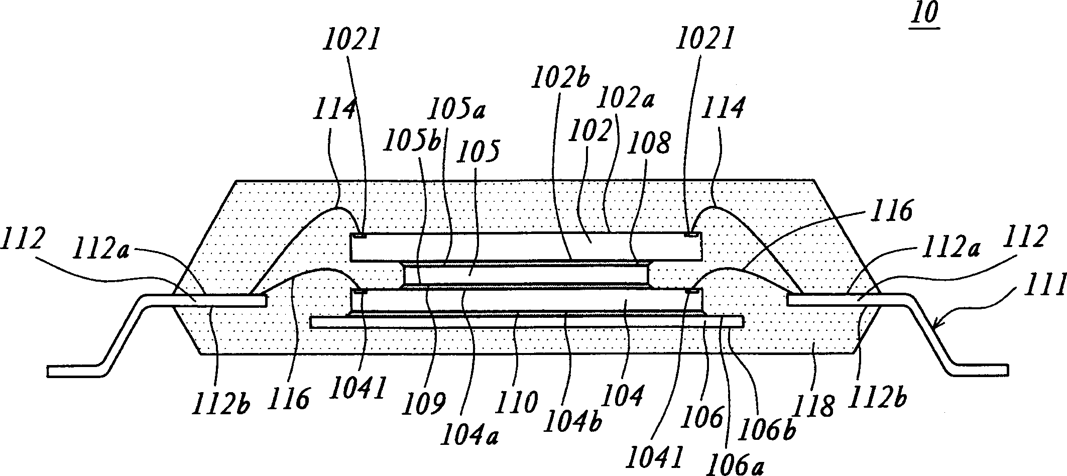
technical field [0001] The present invention relates to a multi-chip packaging structure, and in particular to a multi-chip packaging structure in which two chips with the same or similar dimensions are supported by several chip holders with height differences. Background technique [0002] As far as the current semiconductor packaging technology is concerned, a package of colloid is usually used to cover multiple chips to achieve more than double the capacity or more functional requirements, which is the so-called multi-chip packaging structure. For example, a two-chip package structure can be obtained by combining and packaging two chips with the same or similar size. Wherein, the above-mentioned two chips with the same or similar size may have the same function or different functions. [0003] Please refer to figure 1 , which shows a cross-sectional view of a conventional multi-chip packaging structure. exist figure 1 Among them, the multi-chip package structure 10 in...

Claims


Application Information

Patent Timeline
IPC IPC(8): H01L25/00H01L23/488
CPCH01L2224/05554H01L2224/48091H01L2224/48247H01L2224/73265
Inventor 李睿中李纪纲邱景明
Owner MACRONIX INT CO LTD
Learn More