Liquid crystal display

A liquid crystal display device, liquid crystal technology, applied in optics, instruments, nonlinear optics, etc., can solve the problems of uneven display surface, increased current consumption, residual liquid or smudges on the alignment film, etc., to expand the viewing angle, improve the The effect of speed of response

Inactive Publication Date: 2006-07-12
ALPS ALPINE CO LTD
View PDF2 Cites 15 Cited by
  • Summary
  • Abstract
  • Description
  • Claims
  • Application Information

AI Technical Summary

Problems solved by technology

However, in the case of such a wet alignment process using a resist, there is a problem that liquid or stains remain on the alignment film, and it is impossible to completely remove them from the alignment film.
Therefore, this not only causes unevenness in the display surface, but also increases the current consumption value, and an increase in the current value causes display unevenness during, for example, high-temperature operation.

Method used


Image

  • Liquid crystal display
  • Liquid crystal display
  • Liquid crystal display

Examples


Embodiment 1

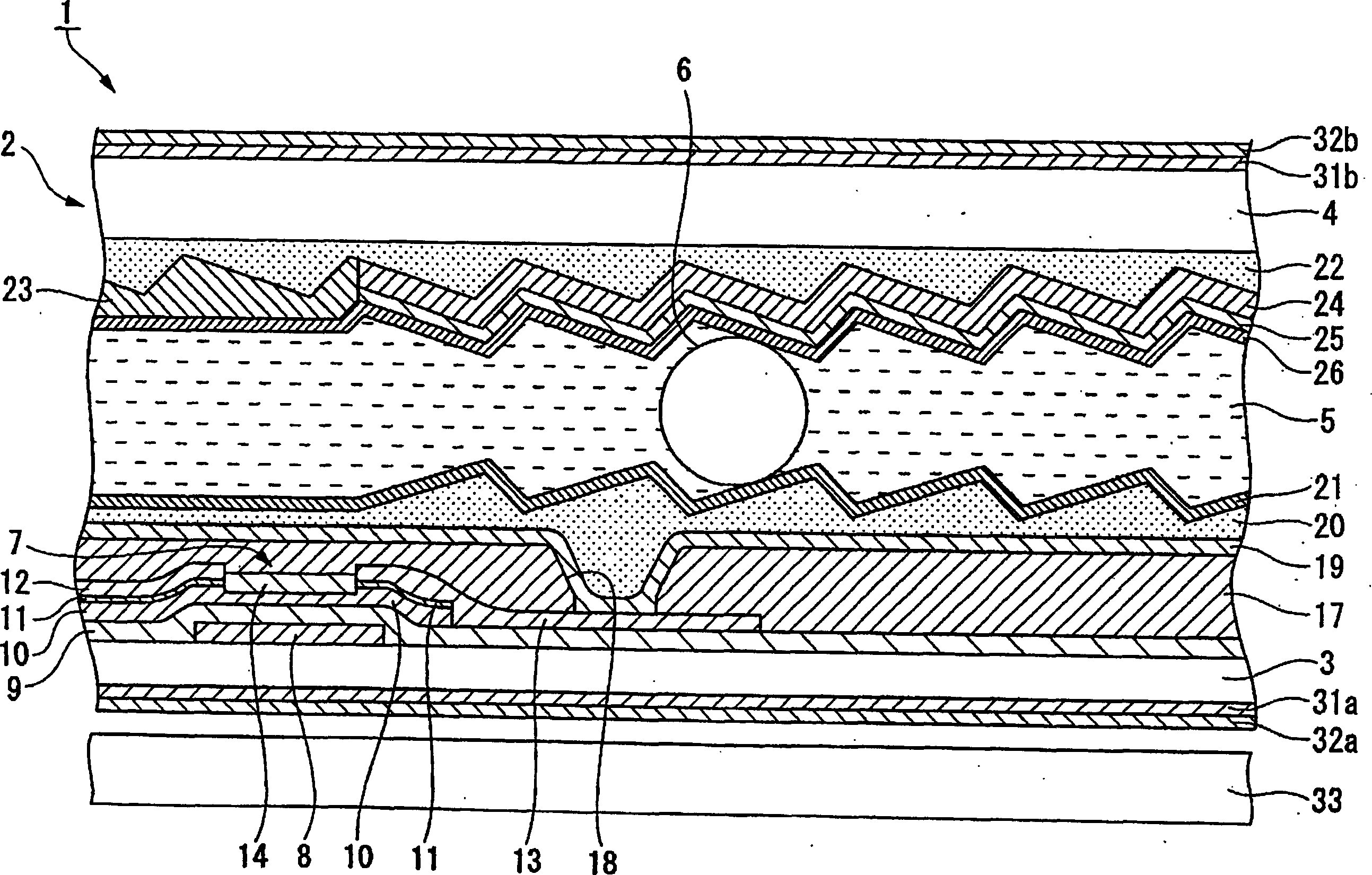
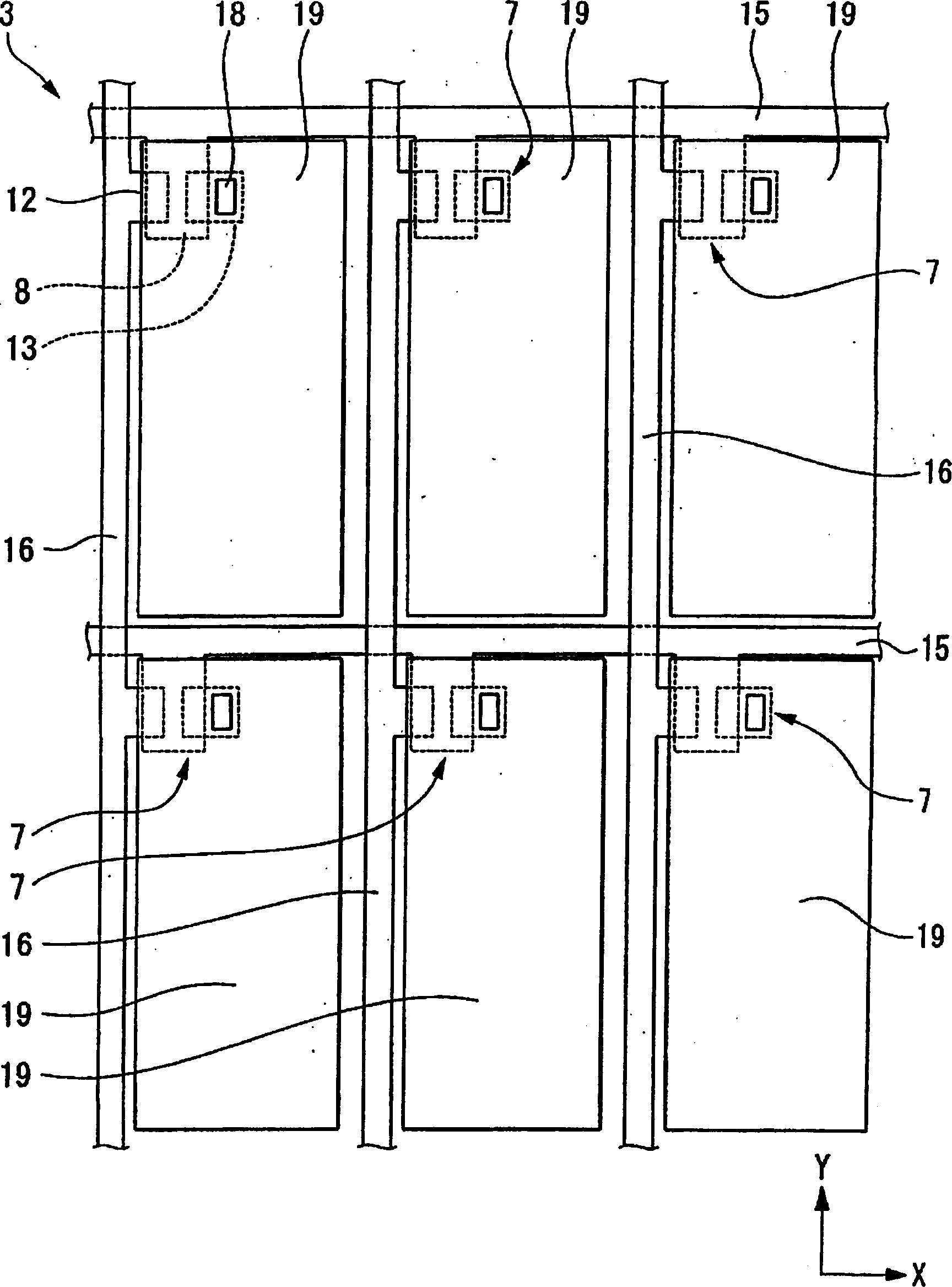
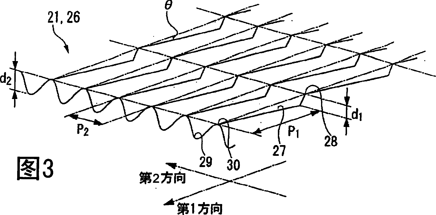
[0051] Example 1 A liquid crystal panel with a diagonal size of about 55 mm (2.2 inches) and a pixel size of 176×128 (XRGB) was fabricated. Specifically, when making the liquid crystal panel, first prepare TFTs, active matrix substrates with scanning lines and signal lines on one main surface side, and form a transparent substrate made of ITO on the active matrix substrates with an insulating film sandwiched between them. the pixel electrode. Next, a photosensitive acrylic resin film is formed on the active matrix substrate, and a replication mold with fine concave-convex shapes to be replicated is formed on the surface and pressed against the film-forming resin layer, and the fine concave-convex shapes are replicated on the active matrix substrate. on the resin layer. In addition, the concavo-convex shape is the same as the shape of the above-mentioned liquid crystal panel 2 shown in FIG. d1 is 0.1 μm. On the other hand, the pitch P2 of the concave-convex shapes repeated i...

Embodiment 2

[0056] Example 2 A liquid crystal panel was produced in the same manner as in Example 1, except that the concentration of γ-methacryloxypropyltrimethoxysilane used for the surface treatment of spacers was 0.1 wt % and 0.3 wt %.

Embodiment 3

[0058] Example 3 A liquid crystal panel was fabricated in the same manner as in Example 1, except that an aqueous solution of γ-glycidoxypropyltrimethoxysilane with a concentration of 0.03 wt% was used for the surface treatment of the spacer material.


PUM

PropertyMeasurementUnit
thicknessaaaaaaaaaa

Abstract

To provide a liquid crystal display device capable of generating the transition of a liquid crystal layer from a splay alignment state to a bend alignment state quickly and stably without applying a high driving voltage.The liquid crystal display device is provided with a liquid crystal panel 2 having: a pair of substrates 3, 4 , which are arranged oppositely to each other and in which electrodes 19, 25 and alignment layers 21, 26 are formed on respective counter surfaces thereof; an OCB mode liquid crystal layer 5 in which a nematic liquid crystal sealed in between the pair of substrates 3, 4 is splay aligned with the alignment layers 21, 26 and the splay aligned nematic liquid crystal is subjected to the transition to the bend aligned state with the driving voltage applied between the electrodes 19, 25; and spacers 6 arranged inside the liquid crystal layer 5 and retaining a gap between the pair of mutually opposing substrates 3, 4 uniform. The spacers 6 are subjected to a surface treatment for accelerating the transition of the liquid crystal layer 5 from the splay aligned state to the bend aligned state.

Description

technical field [0001] The invention relates to an OCB (Optically Compensated Birefringence, Optically Compensated Birefringence) mode liquid crystal display device that realizes large viewing angle and high-speed response characteristics. Background technique [0002] In recent years, a display method called OCB (Optically Compensatory Bend) mode has attracted attention in liquid crystal display devices (for example, refer to Patent Documents 1 and 2). The OCB mode is a liquid crystal panel (II cell) in which the liquid crystal layer sandwiched between a pair of substrates is in a radial alignment state (spray alignment state) and shifts to a bend alignment state when a driving voltage is applied. The optical compensation film of the liquid crystal panel is combined with an optical compensation film, thereby realizing a mode of a large viewing angle and a high response characteristic. However, in this OCB mode, it is not easy to quickly transfer the liquid crystal layer th...

Claims


Application Information

Patent Timeline
Patent Type & Authority Applications(China)
IPC IPC(8): G02F1/1333G02F1/1337
CPCG02F1/133634G02F1/1337G02F1/133711G02F1/1395G02F1/133738
Inventor 林祐三
Owner ALPS ALPINE CO LTD
Why Eureka
Try Eureka