

Method for operating a memory device
一种操作方法、存储区的技术,应用在信息存储、静态存储器、只读存储器等方向,能够解决芯片面积损失、复杂并行参考设计、不利等问题,达到简化脉冲操作步骤、增加可靠性、编程脉冲简单的效果
- Summary
- Abstract
- Description
- Claims
- Application Information
AI Technical Summary
Problems solved by technology
Method used
Image

Examples
Embodiment Construction
[0039] The present invention will be described in further detail below in conjunction with the accompanying drawings.
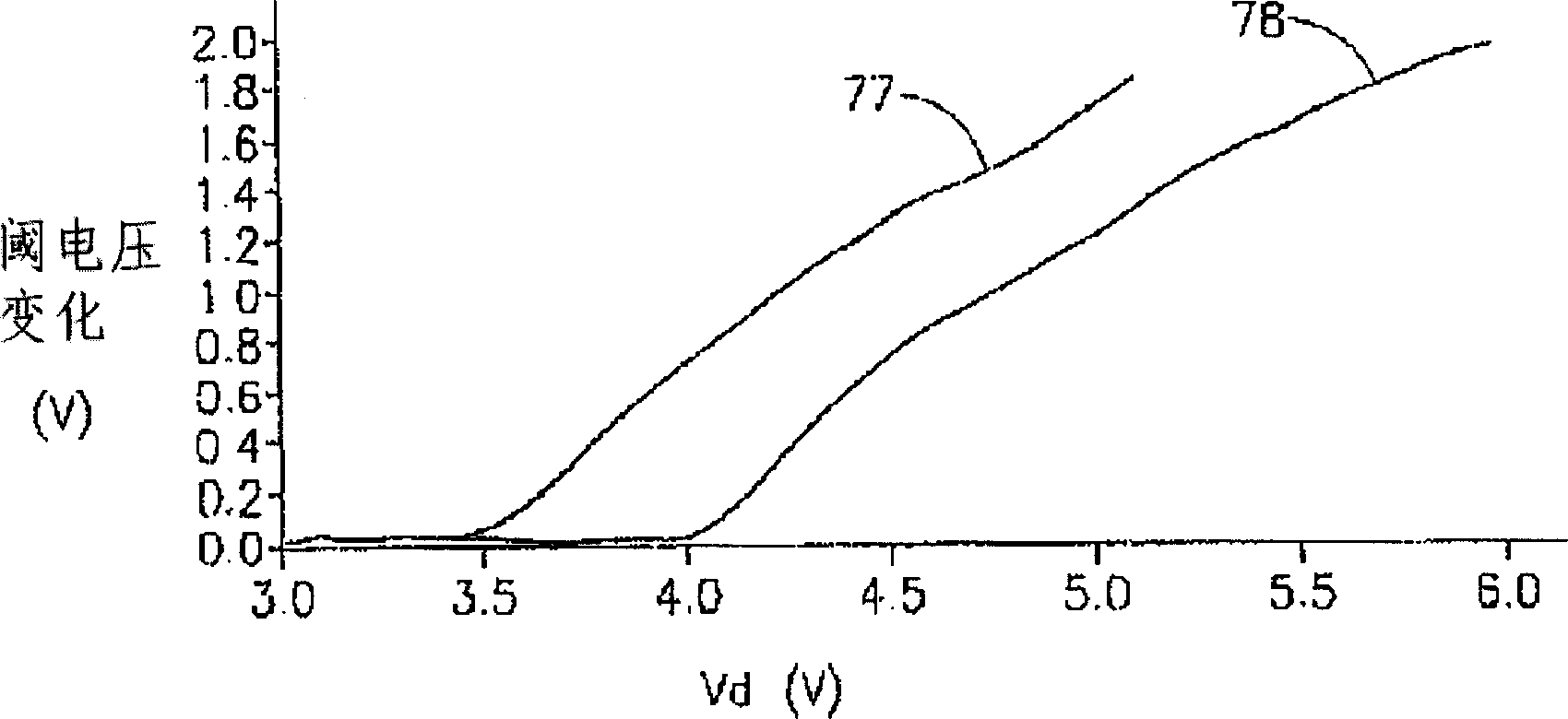
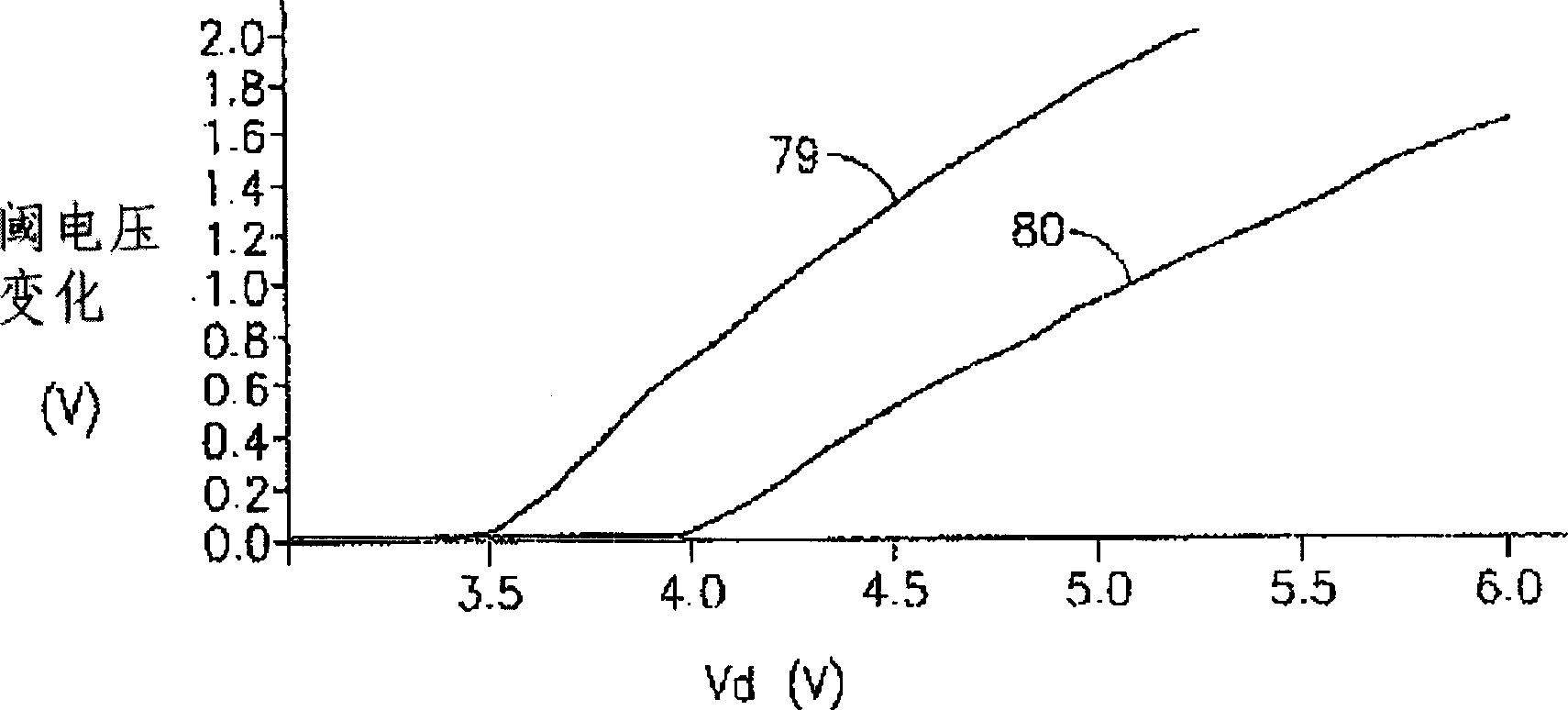
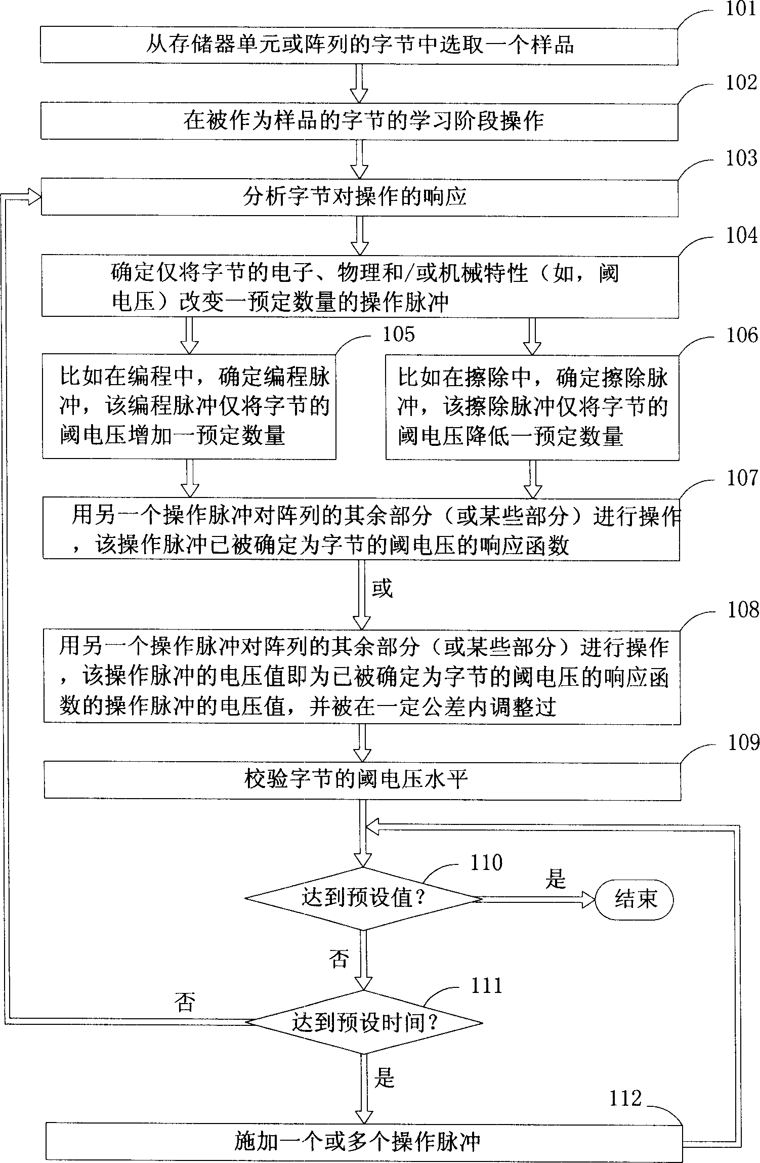
[0040] see image 3 , which shows a method for manipulating memory cell bytes in a memory cell array in one embodiment of the present invention. it's here, image 3 Programming of bytes is shown and described, but it is worth noting that the invention is not limited to programming operations, the invention can also be applied to other operations such as erasing, but is not limited thereto.
[0041] A group of memory cells or array bytes may be selected (step 101). The number of storage units can be selected arbitrarily, such as 64 units, but not limited thereto. The bytes in the group may be programmed (step 102), such as using a step-by-step programming algorithm. The above-mentioned US patent application 09 / 730586, entitled "A Method of Programming and Erasing a NROM Array", describes a suitable step-by-step programming algorithm. The method includes a...
PUM
 Abstract
Description
Claims
Application Information