Method for manufacturing semiconductor device and semiconductor device

A device manufacturing method and semiconductor technology, applied in semiconductor/solid-state device manufacturing, semiconductor devices, semiconductor/solid-state device components, etc., can solve problems such as rewiring damage, side damage, substrate side cut surface exposure, etc., to prevent damage , to ensure the effect of dimensional accuracy

Inactive Publication Date: 2006-09-20
YAMAHA CORP
View PDF2 Cites 13 Cited by
  • Summary
  • Abstract
  • Description
  • Claims
  • Application Information

AI Technical Summary

Problems solved by technology

[0003] However, a conventional WL-CSP (semiconductor device) is divided into individual semiconductor devices by dicing (dicing) the wafer at the final stage, so even if the main surface of the substrate of the semiconductor device (wafer after dicing) is molded with resin, the side surface of the substrate The cut surface is still exposed
The problem is that the exposed sides are prone to damage due to physical impact during the manufacturing steps
[0014] Moreover, in the manufacturing method of the above-mentioned semiconductor device, the first resin layer and the second resin layer covering the side and the back of the substrate are fixed on the side and the back, respectively, so there is a problem that peeling easily occurs due to vibration during dicing, for example.
[0015] The first resin layer covers the side surface and the main surface of the substrate. Therefore, when the first resin layer covering the side surface is peeled off, the first resin layer on the main surface is caused to peel off, and thus, there is an IC formed on the main surface. , rewiring and other damaged problems

Method used


Image

  • Method for manufacturing semiconductor device and semiconductor device
  • Method for manufacturing semiconductor device and semiconductor device
  • Method for manufacturing semiconductor device and semiconductor device

Examples


Embodiment Construction

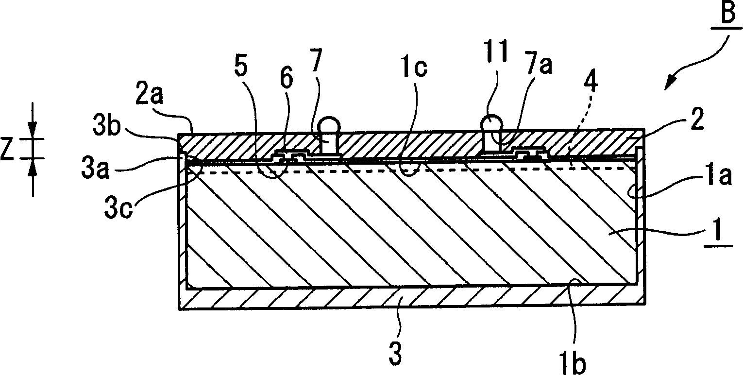
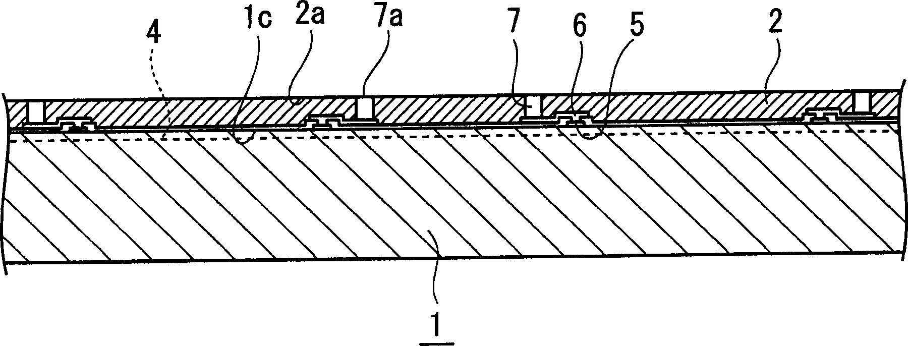
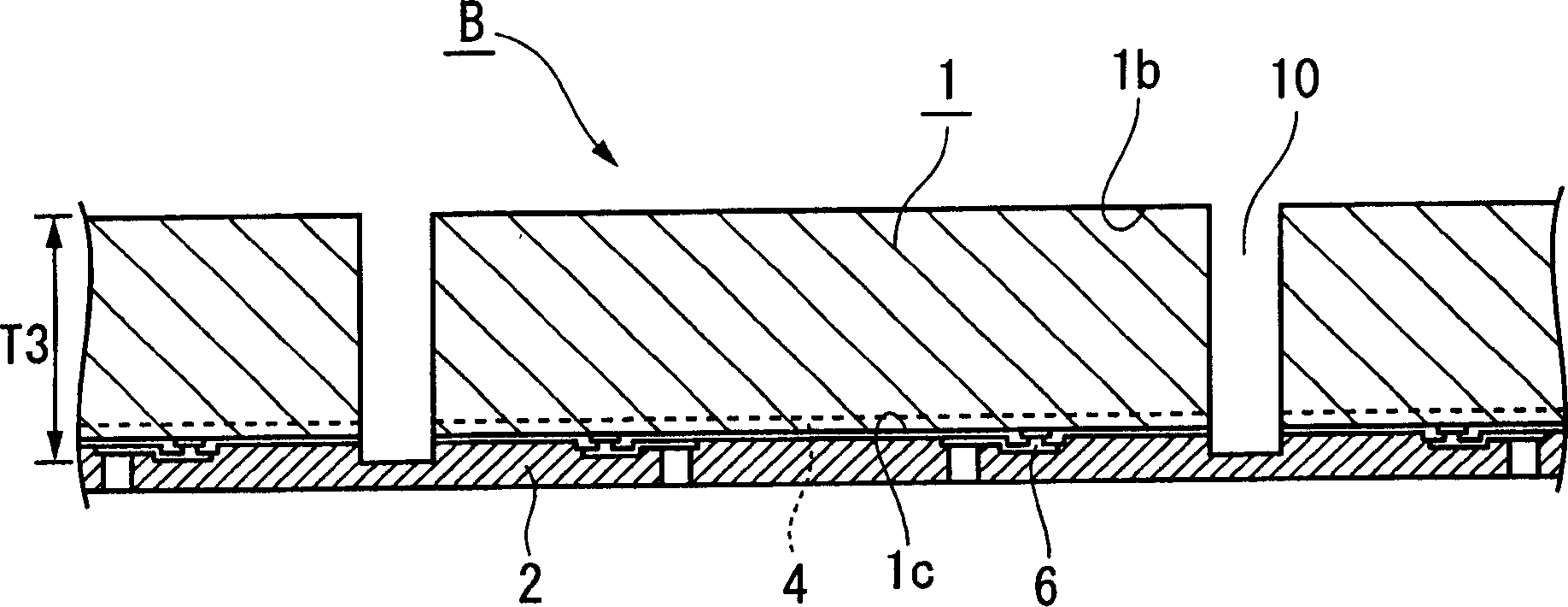
[0073] A semiconductor device B and a manufacturing method thereof according to a first embodiment of the present invention will be described below with reference to the drawings. The semiconductor device B described in this embodiment is mounted and used in devices such as mobile terminal equipment, particularly, in connection with processing wafer-level rewiring and WL-CSP of resin moldings.

[0074] like figure 1 As shown, a semiconductor device B according to the present invention includes: a substrate 1 (wafer after dicing), which is laminated and has an integrated circuit 4 on a main surface 1c; 6; columnar electrode terminals (metal posts) 7 formed on the rewiring 6; first resin layer 2 having a thickness from the main surface 1c of the substrate 1 to the upper surface 7a of the electrode terminals 7 and sealing the main surface 1c of the substrate 1; bumps Electrodes 11 (bumps) are mounted on the upper surface 7 a of the electrode terminal 7 exposed on the surface 2 ...


PUM


Abstract

A semiconductor device production method which includes steps of: preparing a wafer on which multiple integrated circuits are formed on a principal face; forming a rewiring which is electrically connected to the integrated circuits via a pad electrode; and dicing the wafer after forming an electrode terminal on the rewiring, including steps of: forming a first resin layer by sealing at least the rewiring and the electrode terminal formed on the principal face of the wafer with a first resin; processing a first dicing from a back face of the wafer to the principal face of the wafer or halfway to the first resin layer when the first resin layer is formed; forming a second resin layer by sealing a cut line outlined upon the first dicing and the back face of the wafer continuously with a first resin; and processing a second dicing while leaving the second resin layer which covers a side face outlined upon the first dicing.

Description

technical field [0001] The present invention relates to a semiconductor device manufacturing method and a semiconductor device in which packaging is performed at the wafer level and dicing is performed at the final stage. Background technique [0002] In recent years, semiconductor devices applied to devices such as mobile terminals have been required to be small and thin and have faster processing in accordance with demands for increased functions and improved performance of devices such as mobile terminals, for example. A semiconductor device known as a so-called WL-CSP (Wafer Level Chip Scale Package) has attracted attention because it is suitable for such demands. WL-CSP is produced in such a manner that, at the wafer level, rewiring is formed, electrode terminals and resin molds (packages) are formed, and dicing is performed at the final stage, where the resin molds are mainly In order to protect ICs (Integrated Circuits) formed on the main surface of the wafer from he...

Claims


Application Information

Patent Timeline
Patent Type & Authority Applications(China)
IPC IPC(8): H01L21/56H01L23/28
CPCH01L2924/14H01L2224/96
Inventor 中村猛利齐藤博
Owner YAMAHA CORP
Why Eureka
Try Eureka