EL device, manufacturing method of same, and liquid crystal display device using el device

A technology of EL device and manufacturing method, applied in the direction of semiconductor/solid-state device manufacturing, electric solid-state device, semiconductor device, etc.

Inactive Publication Date: 2006-09-20
TOYOTA IND CORP
View PDF1 Cites 9 Cited by
  • Summary
  • Abstract
  • Description
  • Claims
  • Application Information

AI Technical Summary

Problems solved by technology

This is because the light that cannot enter the liquid crystal panel A or the light that cannot be emitted even if it enters the liquid crystal panel A is light that cannot be used as a liquid crystal display device.

Method used


Image

  • EL device, manufacturing method of same, and liquid crystal display device using el device
  • EL device, manufacturing method of same, and liquid crystal display device using el device
  • EL device, manufacturing method of same, and liquid crystal display device using el device

Examples


Embodiment approach 1

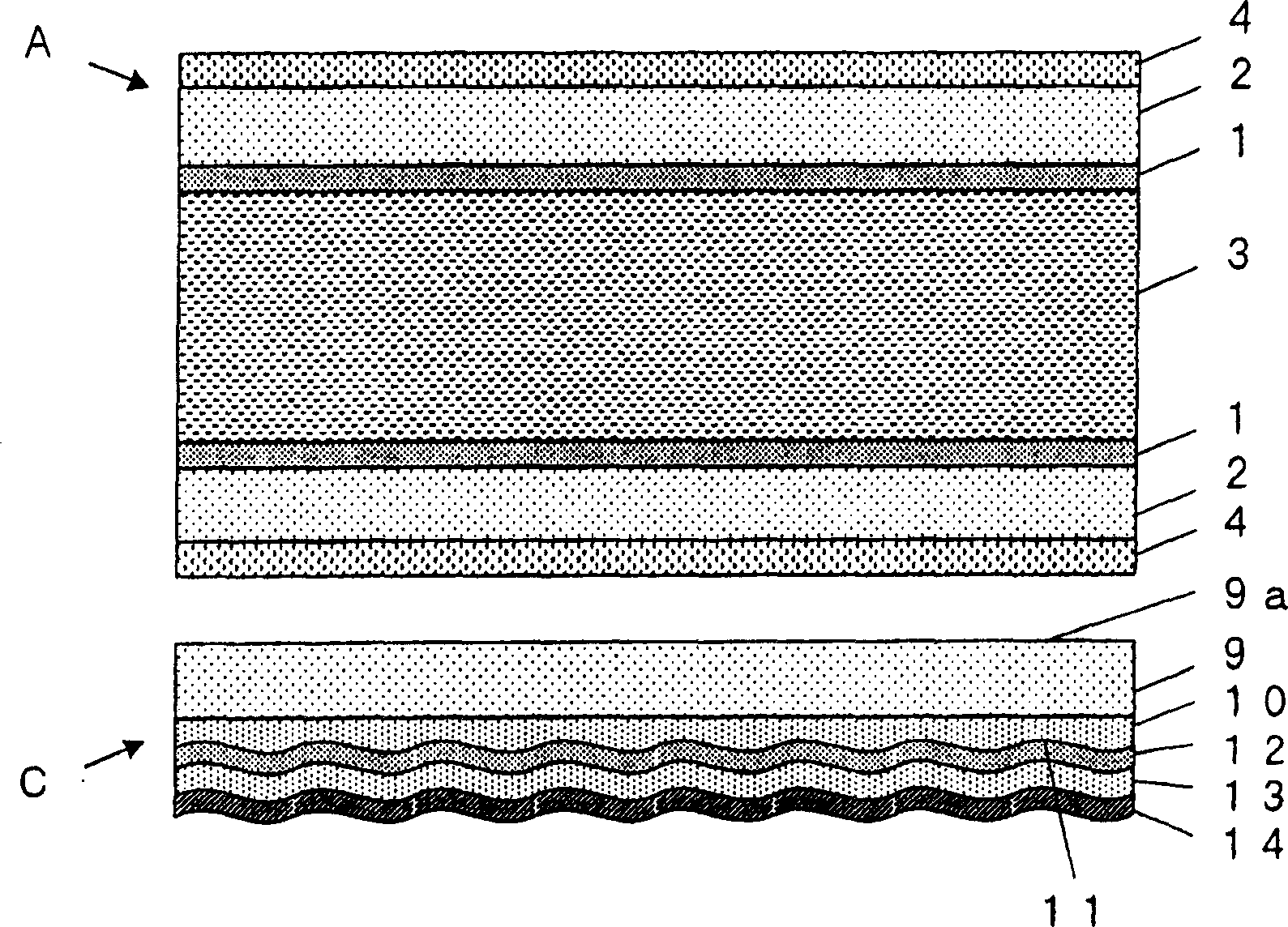
[0048] figure 1 A cross section of the liquid crystal display device of Embodiment 1 is shown. This liquid crystal display device is composed of a liquid crystal panel A and an organic EL device C disposed behind the panel A as a backlight. The liquid crystal panel A has a pair of glass substrates 2 arranged parallel to each other and having transparent electrodes 1 formed on their facing surfaces. Liquid crystal is sealed between the pair of glass substrates 2 to form a liquid crystal layer 3 . Furthermore, polarizing plates 4 are respectively arranged on the outer sides of the pair of glass substrates 2 .

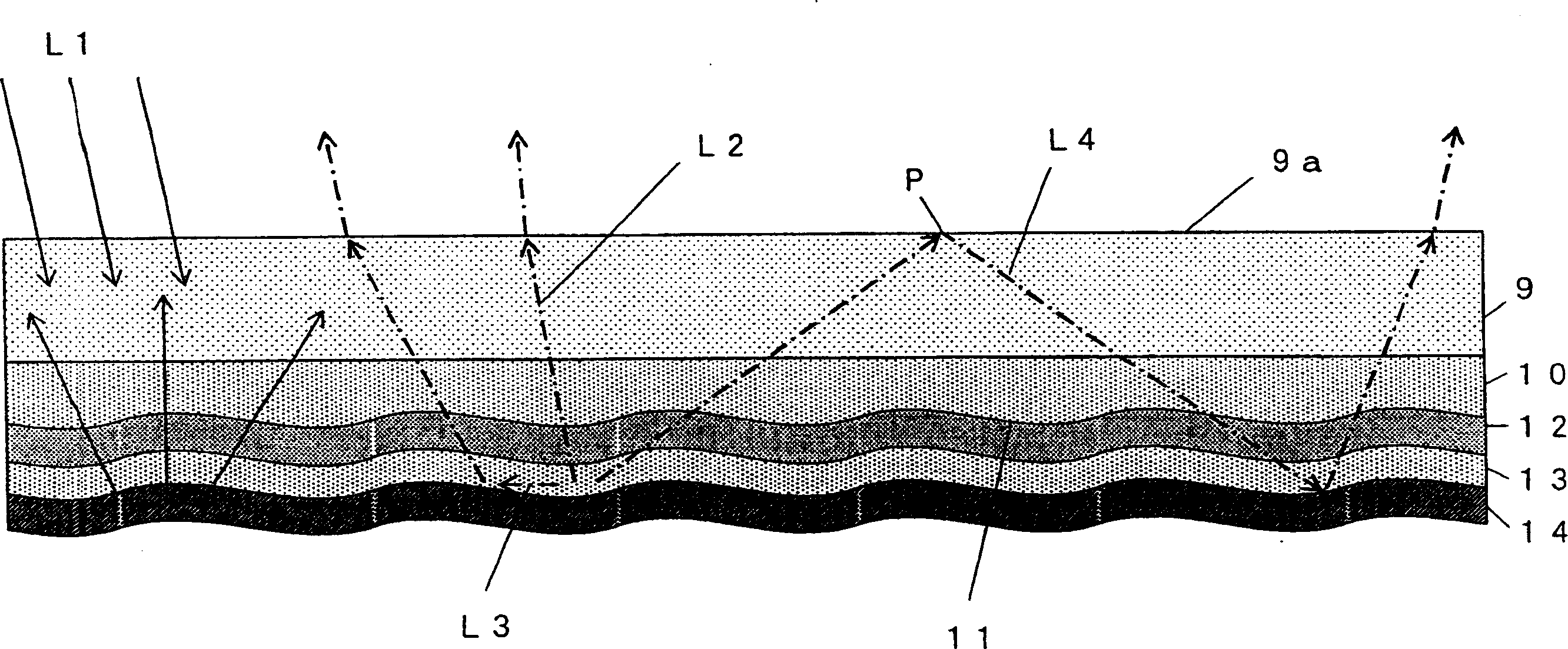
[0049]On the other hand, the organic EL device C has a flat transparent substrate 9 on which the transparent layer 10 constituting the intermediate layer of the present invention is formed. On the surface of the transparent layer 10 opposite to the transparent substrate 9 , a concavo-convex surface 11 in which concave portions and convex portions are irregularly formed...

Embodiment approach 2

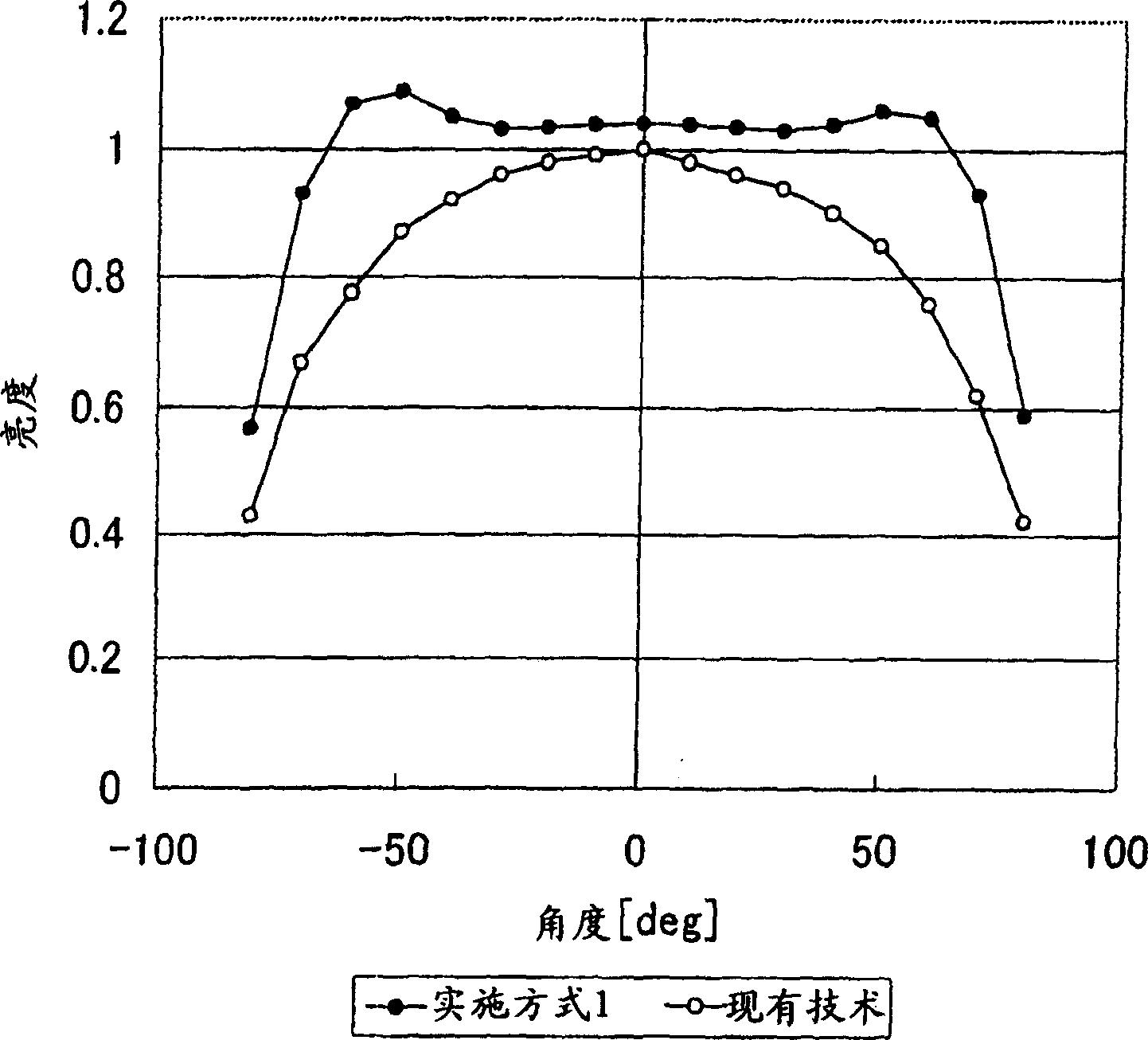
[0070] Figure 5 A cross section of an organic EL device D according to Embodiment 2 is shown. In the organic EL device D of the second embodiment, one prism sheet 21 is disposed on the light emitting surface 9 a of the transparent substrate 9 of the organic EL device C of the first embodiment. here, as Image 6 As shown, the prism sheet 21 has a plurality of linear protrusions 21 a formed parallel to each other. Each linear convex portion 21a has a pointed cross-sectional triangle shape, and by disposing the prism sheet 21 on the light-emitting surface 9a of the transparent substrate 9, the shape of the linear convex portion 21a (the angle of the cross-sectional triangle to the light-emitting surface 9a) Corresponding to the refractive index of the prism sheet 21, the direction of the light emitted from the light exit surface 9a is refracted. For example, if a prism sheet is used that refracts light at an incident angle of about 50 degrees to the normal direction of the li...


PUM


Abstract

An external light L1 impinging on the transparent substrate (9) of an organic EL device and passing through the substrate (9) further passes through a transparent layer (10), a transparent electrode (12) and an organic light emitting layer (13) before being reflected off a reflective electrode (14). Since the reflective electrode (14) has protrusions and recesses, the external light L1 is scattered thereat and reflected at various angles. When passing through the interface between the organic light emitting layer (13) and the transparent electrode (12) and the protruding and recessed surface (11) of the transparent layer (10), these reflected lights are scattered furthermore and exits from the transparent substrate (9) toward the liquid crystal panel. On the other hand, lights L2-L4 emitted from the organic light emitting layer (13) are scattered when they pass through the interface between the organic light emitting layer (13) and the transparent electrode (12) and the protruding and recessed surface (11) of the transparent layer (10), and exits from the transparent substrate (9) toward the liquid crystal panel.

Description

technical field [0001] The present invention relates to an EL (Electroluminescence: electroluminescence) device, particularly an EL device used as a backlight source of a liquid crystal display device. [0002] Moreover, this invention relates to the manufacturing method of such an EL device, and the liquid crystal display device using an EL device. Background technique [0003] Heretofore, EL devices such as inorganic EL devices and organic EL devices have been used as displays or lighting devices. For example, in EL devices used as lighting devices, such as Figure 13 As shown, there is also an organic EL device B arranged behind the liquid crystal panel A as a backlight to constitute a liquid crystal display device. [0004] The liquid crystal panel A has a pair of glass substrates 2 arranged parallel to each other and having transparent electrodes 1 formed on their facing surfaces. Liquid crystal is sealed between the pair of glass substrates 2 to fo...

Claims


Application Information

Patent Timeline
Patent Type & Authority Applications(China)
IPC IPC(8): H05B33/02H05B33/10H05B33/14G02F1/13357G02F1/1335H01L51/52
CPCH01L51/5262G02F1/133611G02F2202/02H01L51/5281H01L2251/5361G02F1/133606H10K50/85H10K50/86H05B33/22H05B33/10
Inventor 内海彻哉舟田真理加藤祥文伊藤日艺竹内范仁
Owner TOYOTA IND CORP
Why Eureka
Try Eureka