Memory subsystem and its method for generating latch clock

A generation method and memory technology, which are applied in static memory, digital memory information, information storage, etc., to ensure the timing and the effect of reading and writing operations.

Active Publication Date: 2006-09-27
MEDIATEK INC
View PDF1 Cites 7 Cited by
  • Summary
  • Abstract
  • Description
  • Claims
  • Application Information

AI Technical Summary

Problems solved by technology

However, it is still possible for this algorithm to select the operating point closest to the edge of the Shmoo graph

Method used


Image

  • Memory subsystem and its method for generating latch clock
  • Memory subsystem and its method for generating latch clock
  • Memory subsystem and its method for generating latch clock

Examples


Embodiment

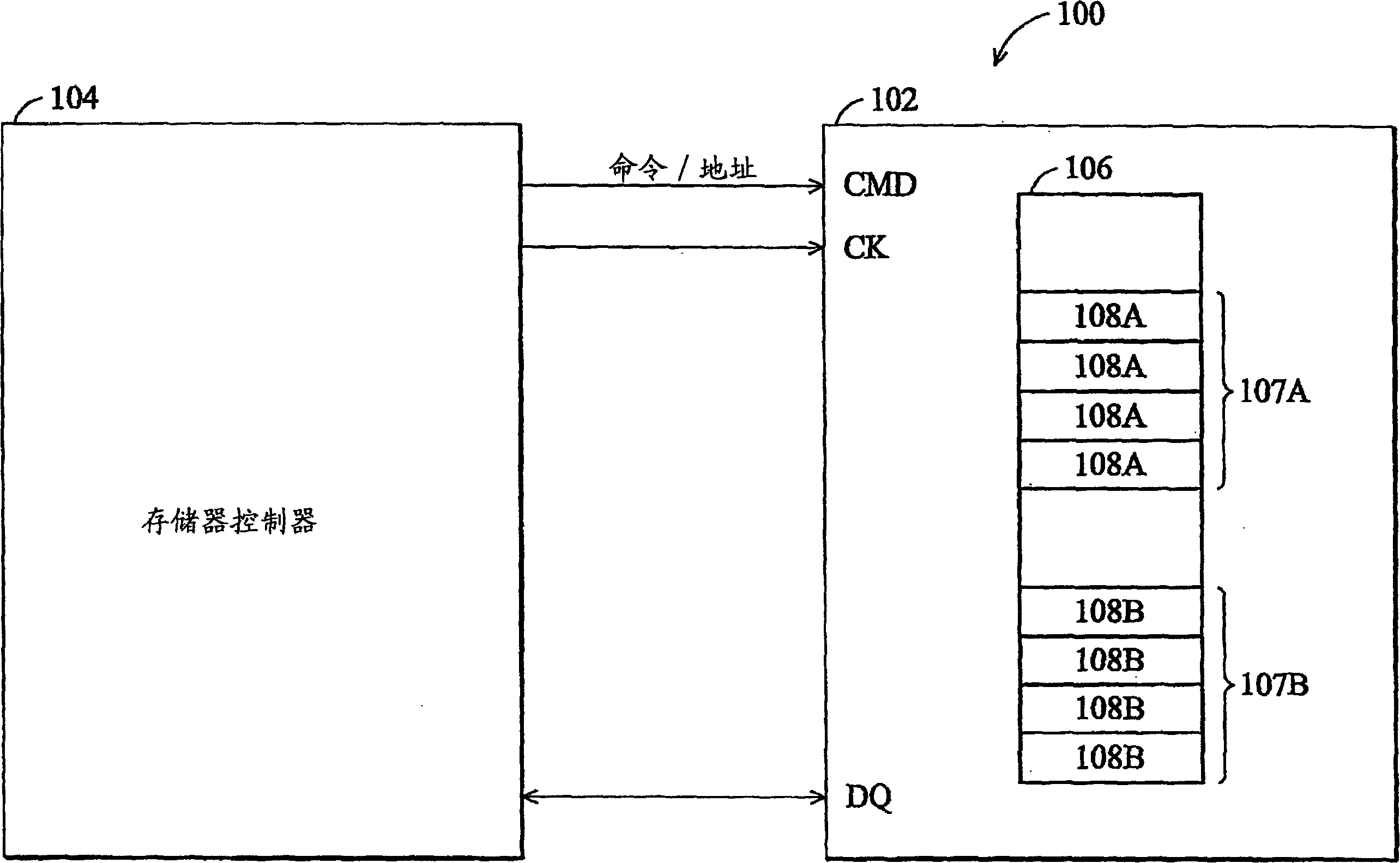
[0036] figure 1 It is a simplified functional block diagram showing a memory subsystem 100 according to an embodiment of the present invention, including a memory controller 104 and a memory 102 . The memory 102 typically has a memory array 106 of multiple banks. figure 1 The memory array 106 is shown as an example of two sets of banks 107A and 107B. The memory array 106 also includes a plurality of memory elements (not shown) for storing data, and the memory elements are generally arranged in addressable rows and columns respectively. Those skilled in the art typically refer to a commonly addressable subset of memory array 106 as a memory page. In general, memory cells in the same column within a bank in the memory array 106 constitute a particular memory page. exist figure 1 A plurality of memory pages (labeled 108A and 108B) corresponding to banks 107A and 107B, respectively, are shown.

[0037] Those skilled in the art understand that specific locations in memory arra...


PUM


Abstract

Methods and systems for generating a latch clock in memory reading. Data with a first logic level and with a second logic level are stored into a first address and a second address of a memory, respectively. A read data signal is generated by issuing continuous read commands for repeated retrieval of the data at the first and the second addresses of the memory. A divided frequency signal is generated by dividing a frequency of the internal clock. A phase of the divided frequency signal is adjusted according to a delay parameter by varying the delay parameter until at least an edge of the divided frequency signal is aligned with any edge of the read data signal. Finally, the latch clock is generated according to the delay parameter and the internal clock.

Description

technical field [0001] The present invention relates to a memory subsystem, and more particularly to a method and system for generating a latch clock for reading memory. Background technique [0002] In many random access memory (RAM) architectures, two common forms of volatile RAM are dynamic random access memory (DRAM) and static random access memory (static random access memory). , SRAM). Each storage unit (or bit) of the SRAM is composed of a flip-flop, and a basic storage device usually requires about six transistors. In contrast, each bit of DRAM requires only one transistor, so DRAM is usually cheaper and more compact than SRAM. SRAM is generally faster than DRAM and easier to operate. Thus, SRAM is typically used in faster but smaller memory computing devices, while DRAM is typically used in computing devices requiring large amounts of random access memory. In fact, many microprocessor-based systems use a combination of DRAM and SRAM. DRAM chips are used to form ...

Claims


Application Information

Patent Timeline
Patent Type & Authority Applications(China)
IPC IPC(8): G11C7/22
CPCG11C29/02G11C7/1072G11C7/22G11C7/222G11C11/4076G11C29/023G11C29/028G11C2207/2254
Inventor 曾瑞兴
Owner MEDIATEK INC
Why Eureka
Try Eureka