Optical recording medium
An optical recording medium and recording layer technology, which is applied in the directions of data recording, temperature recording, recording/reproducing by optical methods, etc., can solve the problems such as the inability to obtain the effect and the lack of the medium structure of the low thermal conductivity layer.
- Summary
- Abstract
- Description
- Claims
- Application Information
AI Technical Summary
Problems solved by technology
Method used
Image
Examples
Embodiment 1
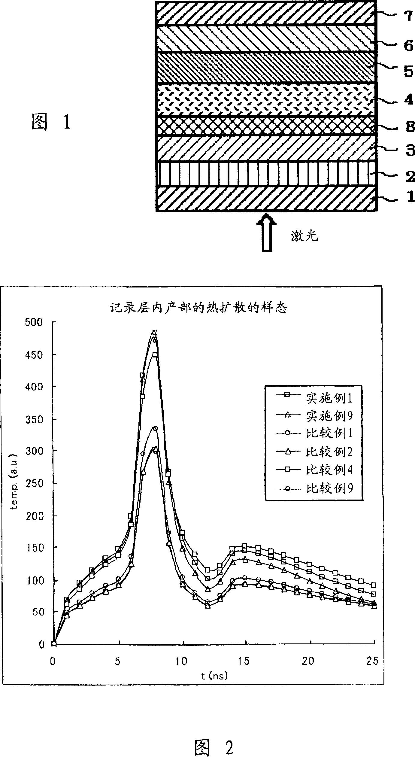
[0123] On the substrate 1, a first protective layer 2, a phase change recording layer 3, a second protective layer 8, a low thermal conductivity layer 4, and a reflective layer 5 are sequentially formed by sputtering, and a resin protective layer 6 is formed on it by a spin coating method. , and finally, the bonding substrate 7 is bonded, and an optical recording medium having the layer structure shown in FIG. 1 is produced and initialized.
[0124] As the substrate 1 , a polycarbonate substrate having a diameter of 12 cm and a thickness of 0.6 mm and a track pitch of 0.74 μm with guide grooves was used.
[0125] The first protective layer 2 uses ZnS-SiO with a thickness of 60nm 2 (80:20 mol%) (κ8.6W / m·K).
[0126] The phase change recording layer 3 uses Ga with a thickness of 16nm 12 Sb 88 .
[0127] The second protective layer 8 uses ZnSSiO with a thickness of 7nm 2 (80:20 mole %).
[0128] Low thermal conductivity layer 4 uses ZrO with a thickness of 4nm 2 (contains...
Embodiment 2
[0140] In addition to changing the material of the low thermal conductivity layer 4 to ZrO 2 (contains 3 mol% Y 2 o 3 )-20mol%TiO 2 Except for the point of (κ2.0W / m·K), an optical recording medium was fabricated and initialized in the same manner as in Example 1, and then evaluated.
Embodiment 3
[0142] In addition to changing the material of the low thermal conductivity layer 4 to ZrO 2 (contains 3 mol% Y 2 o 3 )-10 mol% SiO 2 Except for the point of (κ3.5W / m·K), an optical recording medium was fabricated and initialized in the same manner as in Example 1, and then evaluated.
PUM
| Property | Measurement | Unit |
|---|---|---|
| thermal conductivity | aaaaa | aaaaa |
| thermal conductivity | aaaaa | aaaaa |
| thickness | aaaaa | aaaaa |
Abstract
Description
Claims
Application Information
