Light source

A technology of light source and generating source, applied in the field of light source, can solve the problems of high voltage application, high manufacturing cost, lack of practicability, etc., and achieve the effects of low voltage, improved linear propagation, and reduced crosstalk

Inactive Publication Date: 2006-11-01
NGK INSULATORS LTD
View PDF4 Cites 0 Cited by
  • Summary
  • Abstract
  • Description
  • Claims
  • Application Information

AI Technical Summary

Problems solved by technology

[0003] Conventional examples of this electron emission element include, for example, Patent Documents 1 to 5. However, since no dielectric is used in the emitter, there is a problem that molding or microfabrication must be performed between facing electrodes. , and a high voltage must be applied for electron emission, in addition, the panel manufacturing process is complicated and the manufacturing cost is high
[0013] However, there are problems in that electron emission is unstable, and the number of electron emission is as high as about tens of thousands of times, for example, it lacks practicality when used as a light source

Method used


Image

  • Light source
  • Light source
  • Light source

Examples


Embodiment Construction

[0159] Refer to the following Figure 1 to Figure 77 Examples of the light source of the present invention will be described.

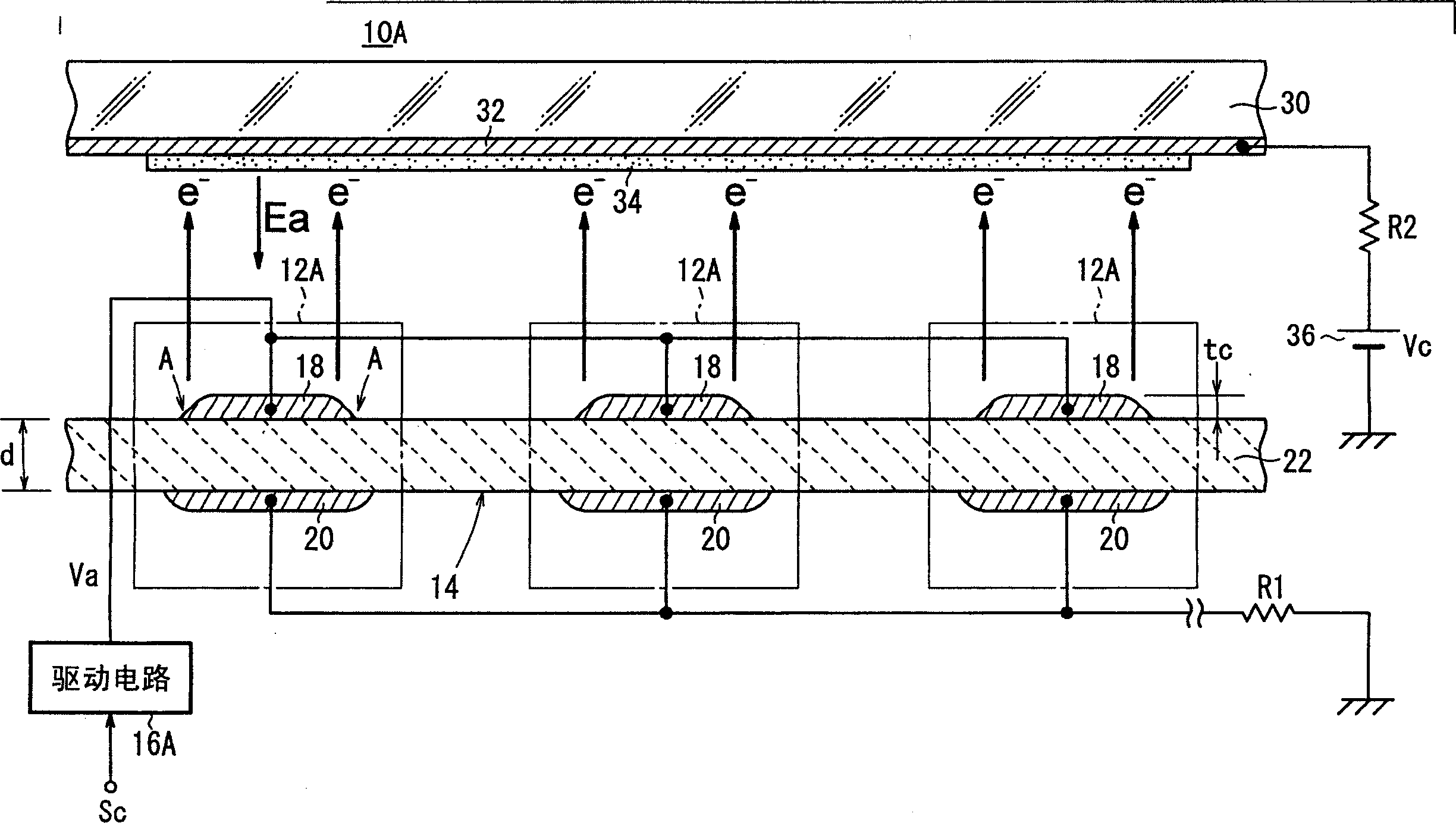
[0160] Such as figure 1 As shown, the light source 10A of the first embodiment has a light emitting section 14A in which a plurality of electron emitting elements 12A are arranged two-dimensionally, and a drive circuit 16A for applying a driving voltage va to each electron emitting element 12A of the light emitting section 14A.

[0161] The driving circuit 16A applies a driving voltage Va to the first electrode (for example, the upper electrode) 18 and the second electrode of each electron emission element 12A according to a control signal Sc indicating turning on / off the light from the outside (a light-on / off switch, etc.). On the (lower electrode) 20, each electron emission element 12A is driven and controlled. A preferred example of the drive circuit 16A will be described later.

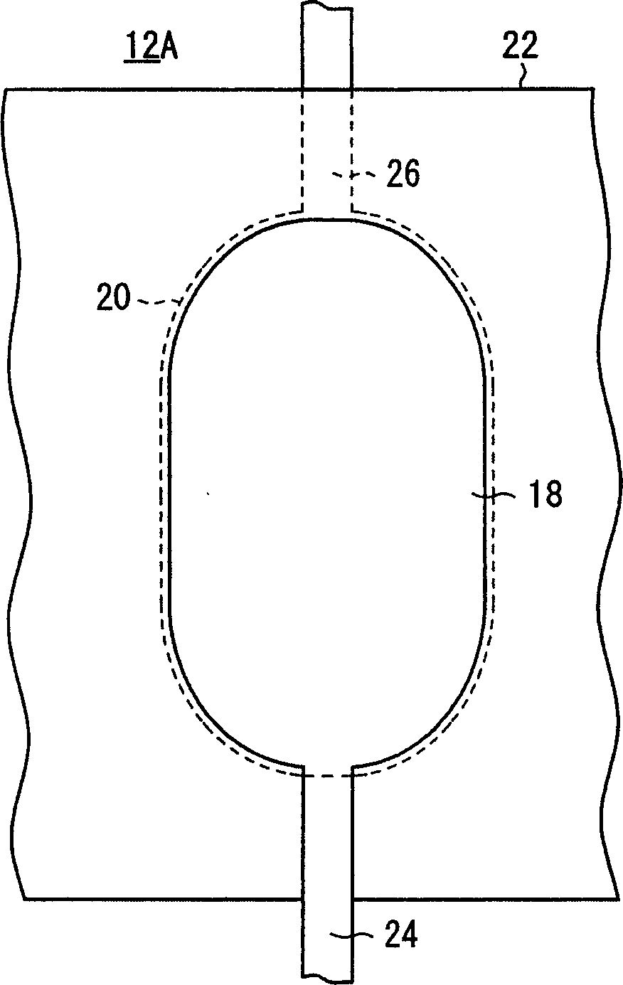
[0162] Such as figure 1 As shown, each electron emission element...


PUM


Abstract

A light resource has a light emitting unit that consists of plural electron emitting elements arranged in two dimensions. Control signals make driving circuits to supply working voltage onto the said electron emitting elements consisting of an planar emitting body, and upper electrodes on the top of the planar emitting body and lower electrodes on the back of the planar emitting body.

Description

technical field [0001] The present invention relates to a light source (including a surface light source) using an electron emission element having an upper electrode and a lower electrode formed on an emitter. Background technique [0002] Recently, electron emission elements are being used in various applications such as field emission displays (FED) having driving electrodes and common electrodes or backlights. When used in an FED, a plurality of electron emission elements are arranged two-dimensionally, and a plurality of phosphors facing the electron emission elements are respectively arranged at predetermined intervals. [0003] Conventional examples of this electron emission element include, for example, Patent Documents 1 to 5. However, since no dielectric is used in the emitter, there is a problem that molding or microfabrication must be performed between facing electrodes. , and a high voltage must be applied for electron emission. In addition, the panel manufactu...

Claims


Application Information

Patent Timeline
Patent Type & Authority Applications(China)
IPC IPC(8): H01J1/312G09G3/20G09G3/22H01J63/02
CPCG09G3/22B82Y10/00H01J1/312H01J63/02
Inventor 武内幸久七泷努大和田岩赤尾隆嘉
Owner NGK INSULATORS LTD
Why Eureka
Try Eureka