Transistor including metal-insulator transition material and method of manufacturing the same

A technology for converting materials and insulators, applied in transistors, semiconductor/solid-state device manufacturing, electric solid-state devices, etc., can solve problems such as device unreliability, heating speed, and reduction

Inactive Publication Date: 2006-11-15
SAMSUNG ELECTRONICS CO LTD
View PDF0 Cites 4 Cited by
  • Summary
  • Abstract
  • Description
  • Claims
  • Application Information

AI Technical Summary

Problems solved by technology

Therefore, an increase in gate insulating layer capacitance causes problems such as heat generation and speed reduction
However, if the capacitance is low, the device becomes less reliable due to leakage current

Method used


Image

  • Transistor including metal-insulator transition material and method of manufacturing the same
  • Transistor including metal-insulator transition material and method of manufacturing the same
  • Transistor including metal-insulator transition material and method of manufacturing the same

Examples


Embodiment Construction

[0029] The present invention will be described more fully hereinafter with reference to the accompanying drawings, in which exemplary embodiments of the invention are shown. In the drawings, the size and thickness of layers and regions are exaggerated for clarity.

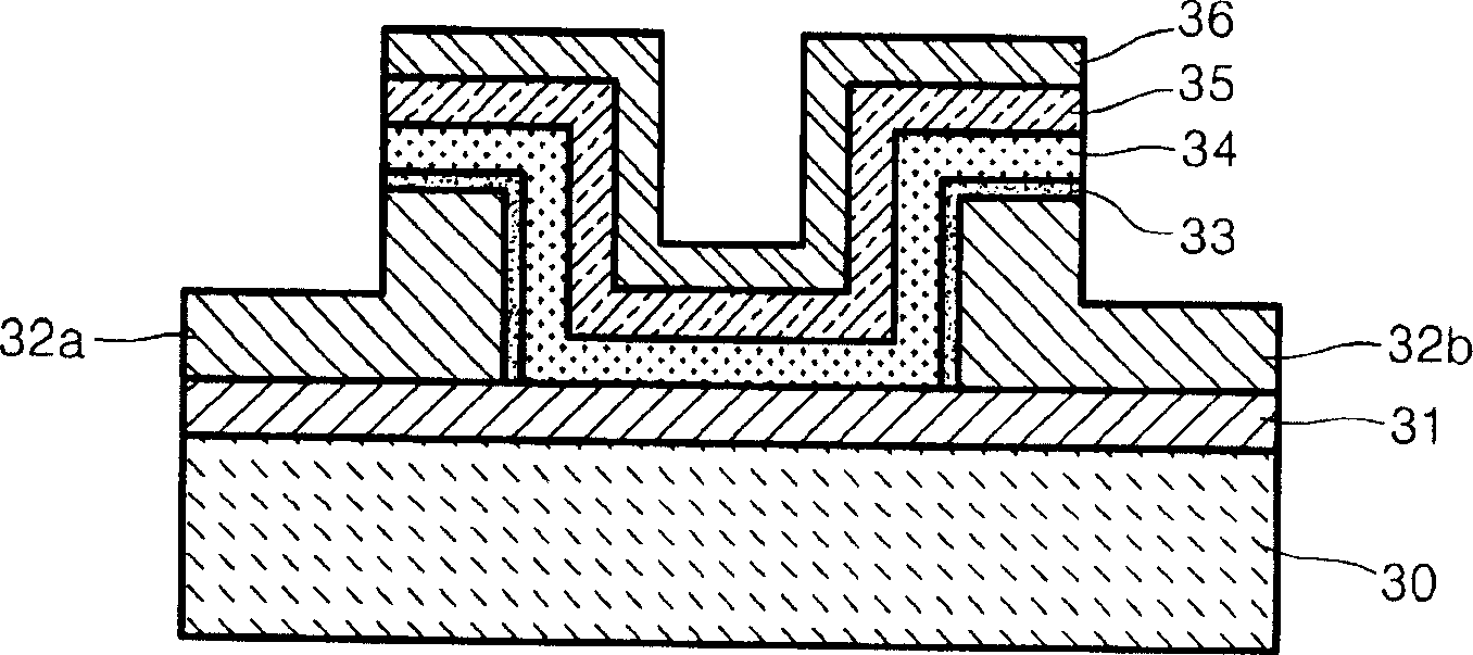
[0030] figure 1 is a cross-sectional view of a transistor using a metal-insulator conversion material according to an embodiment of the present invention. refer to figure 1 , forming an insulating layer 31 on the substrate 30 . The first and second conductive patterns 32a and 32b are formed on the insulating layer 31 and separated from each other. One of the first and second conductive patterns 32a and 32b serves as a source region, and the other serves as a drain region. Hereinafter, the first conductive pattern 32a is referred to as a source region, and the second conductive pattern 32b is referred to as a drain region. A tunnel barrier layer 33 is formed on each of the source region 32a and the drain region...


PUM


Abstract

A transistor including a metal-insulation transition material and a method of manufacturing the same. The transistor including a metal-insulator transition material may include a substrate, a insulation layer formed on the substrate, a source region and a drain region separately formed from each other on the insulation layer, a tunneling barrier layer formed on at least one surface of the source region and the drain region, a metal-insulator transition material layer formed on the tunneling barrier layer and the insulation layer, a dielectric layer stacked on the metal-insulator transition material layer, and a gate electrode layer formed on the dielectric layer.

Description

technical field [0001] The present invention relates to a semiconductor device and its manufacturing method, and more particularly, to a transistor including a metal insulator conversion material and its operation and manufacturing method, wherein in order to reduce the leakage current between the source region and the drain region A tunneling barrier layer is formed between them. Background technique [0002] With the development of semiconductor technology, highly integrated semiconductor devices are increasingly required. In order to highly integrate semiconductor devices, it is necessary to reduce the size of field effect transistors (FETs) therein. However, many technical issues may arise. [0003] The smaller the field effect transistor (FET), the shorter the channel length between the source region and the drain region, thus causing the short channel effect. The short channel effect excessively reduces the threshold voltage of the FET and also reduces the carrier m...

Claims


Application Information

Patent Timeline
Patent Type & Authority Applications(China)
IPC IPC(8): H01L29/78H01L21/336
CPCH10N99/03H01L29/788H01L29/792H10N70/00H10N70/231H10N70/882H10N70/011
Inventor 赵重来柳寅儆崔梁圭赵成逸
Owner SAMSUNG ELECTRONICS CO LTD
Why Eureka
Try Eureka