Fringe field switching mode LCD having high transmittance

A technology of liquid crystal display devices and fringe field switches, applied in nonlinear optics, instruments, optics, etc., can solve uneconomical problems and achieve the effect of increasing transmittance and reducing horizontal distance

Inactive Publication Date: 2006-12-20
BOE HYDIS TECH CO LTD
View PDF1 Cites 8 Cited by
  • Summary
  • Abstract
  • Description
  • Claims
  • Application Information

AI Technical Summary

Problems solved by technology

[0014] However, the reduction of the l' value for increasing such an average overall transmittance is difficult to form in the actual process due to the fineness of the l' value, so it is not economical.

Method used


Image

  • Fringe field switching mode LCD having high transmittance
  • Fringe field switching mode LCD having high transmittance
  • Fringe field switching mode LCD having high transmittance

Examples


Embodiment Construction

[0030] The best mode for carrying out the present invention will be described in detail below with reference to the accompanying drawings.

[0031] First of all, in the FFS mode liquid crystal display device, the lower substrate is bonded to the upper substrate with the liquid crystal layer interposed. The lower substrate has such a structure that gate bus lines and data bus lines are cross-arranged to form a unit pixel. In the unit pixel area A count electrode and a pixel electrode are disposed with a gate insulating film interposed therebetween; the upper electrode corresponds to each pixel region and has a color film. The above content is the content of the prior art, so the accompanying drawings are omitted.

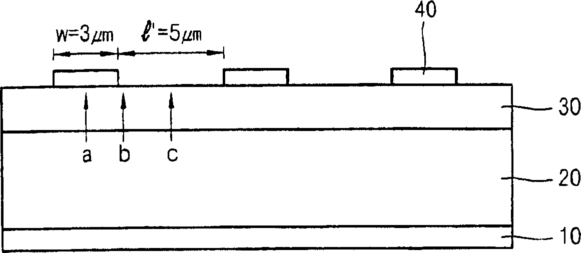
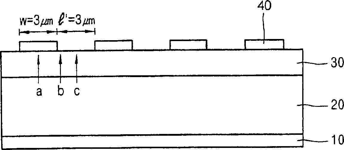
[0032] Figure 5 It is a schematic array cross-sectional view showing an FFS mode liquid crystal display device according to an embodiment of the present invention.

[0033] Referring to the drawings, a schematic array of an FFS mode liquid crystal display device i...


PUM

PropertyMeasurementUnit
widthaaaaaaaaaa

Abstract

Provided is a fringe field switching mode LCD having altered pixel electrodes configuration to easily increase the overall transmittance. A fringe field switching mode LCD includes a lower substrate having a gate bus line and a data bus line arranged to cross each other and form unit pixels and a counter electrode and a pixel electrode positioned within each unit pixel region with a gate insulator interposed between them and an upper substrate provided with a color filter corresponding to each pixel region and bonded to the lower substrate with a liquid crystal layer interposed between them. The pixel electrode includes first pixel electrodes positioned on the gate insulator and second pixel electrodes positioned on a protective layer, which is interposed between the first and second pixel electrodes, with a predetermined horizontal spacing from the respective first pixel electrodes and electrically connected to the first pixel electrodes via contact holes formed on the protective layer.

Description

technical field [0001] The invention relates to a fringe field switch mode liquid crystal display device, in particular to a fringe field switch mode liquid crystal display device with high transmittance. Background technique [0002] The fringe field switching mode (FFS mode) liquid crystal display device is proposed to improve the low aperture ratio and transmittance of the IPS mode (in-plane switching mode) liquid crystal display device. It is registered in the Korean Patent No. 10- Disclosed in No. 0341123. [0003] Such an FFS mode liquid crystal display device uses a transparent conductor to form the counting electrode and pixel electrode. Compared with the IPS liquid crystal display device, the aperture ratio and transmittance are improved, and the interval between the counting electrode and the pixel electrode is formed narrower than that of the upper and lower parts. The gap between the glass substrates forms a fringe field between the counter electrode and the pix...

Claims


Application Information

Patent Timeline
Patent Type & Authority Applications(China)
IPC IPC(8): G02F1/1343G02F1/136
CPCG02F2001/134372G02F1/134363G02F1/134372G02F1/1343
Inventor 朴准伯金香律郑然鹤
Owner BOE HYDIS TECH CO LTD
Why Eureka
Try Eureka