
Single-segment and multi-segment triggering type voltage-adjustable static-electricity discharging protection semiconductor structure

An electrostatic discharge protection and triggering technology, which is applied in the direction of semiconductor devices, semiconductor/solid-state device components, electric solid-state devices, etc., can solve problems such as component damage, damage to electrostatic discharge protection functions, and excessive secondary breakdown voltage

Active Publication Date: 2007-01-10
SYST GEN
View PDF0 Cites 4 Cited by
  • Summary
  • Abstract
  • Description
  • Claims
  • Application Information

AI Technical Summary

Problems solved by technology

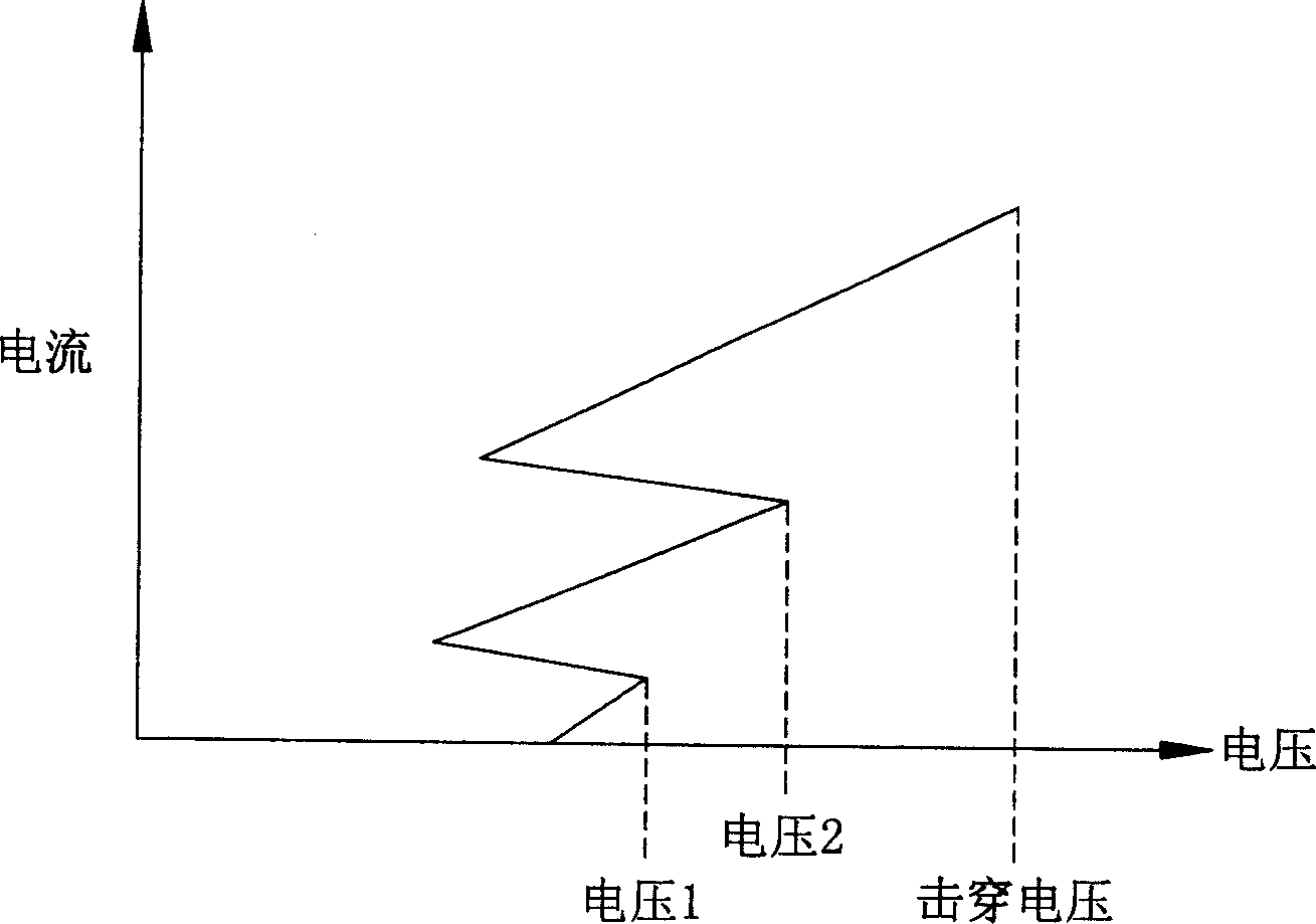
[0002] Electrostatic discharge protection circuits (ESD protection circuits) are specially used for electrostatic discharge protection on integrated circuits. ESD protection components face secondary breakdown after the primary breakdown point when the electrostatic discharge energy continues to increase. point, due to its high secondary breakdown voltage or secondary breakdown current, it will damage the components and destroy the electrostatic discharge protection function
[0003] The PN junction in BJT (Bipolar junction transistor) is used as an electrostatic discharge protection element, and its secondary breakdown trigger breakdown is often dominated by voltage, which means that at the primary breakdown point After that, if the electrostatic discharge energy continues to increase, the voltage and current rise of the component will often trigger the secondary breakdown voltage first, resulting in component damage

Method used


Image

  • Single-segment and multi-segment triggering type voltage-adjustable static-electricity discharging protection semiconductor structure
  • Single-segment and multi-segment triggering type voltage-adjustable static-electricity discharging protection semiconductor structure
  • Single-segment and multi-segment triggering type voltage-adjustable static-electricity discharging protection semiconductor structure

Examples


Embodiment Construction

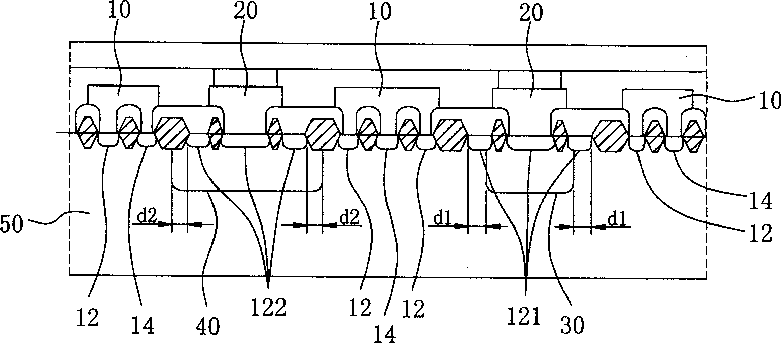
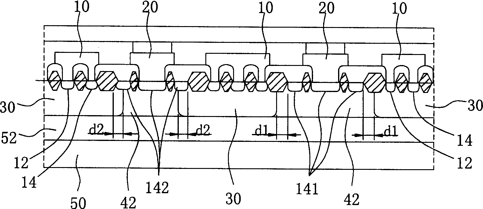
[0031] Please refer to Figure 1 to Figure 3 It is an embodiment and a characteristic diagram of the present invention, in which a plurality of N-well regions or P-well regions are mainly used to form a specific impedance in a P-type substrate to form a breakdown discharge current energy for a specific voltage, and make each well region The discharge capacity is adjustable and connected in parallel to form a multi-stage trigger type electrostatic protection semiconductor structure. (The base material is a larger area material, the well area is a sub-large area material, and the diffusion area is a small area material)

[0032] Please refer to figure 2 and image 3 is an embodiment of the present invention, where figure 2It mainly includes: P-type substrate 50, on which a plurality of electrostatic protection elements are formed, which includes (generally the surface where the substrate is stacked up) (an application example of a semiconductor can be used to protect power ...


PUM


Abstract

Static discharging structure for protecting semiconductor possesses multi sectional function for protecting semiconductor circuit, and adjustable discharge capacity. Advantages are that the invention is easy to accord with current procedure for fabricating semiconductor; the invention can be used in areas of designing and fabricating semiconductor of IC. Using multiple N trap area or P trap area in P type basic material mainly, the invention adjusts discharge capacity in each trap area, and connects each trap area in parallel in order to improve capacity of electrostatic protection and reach dynamic design accorded to semiconductor circuit in different specifications of power. Comparing with well-known circuit of static protection, the invention possesses stronger protection functions: improving protection function for important semiconductor component; making component not easy to be damaged; and providing multiple protections for semiconductor component in high power.

Description

technical field [0001] The present invention relates to a single-segment or multi-segment trigger voltage adjustable electrostatic discharge protection semiconductor structure, which includes using multiple N-well regions or P-well regions in a P-type substrate to adjust the discharge capacity of each well region and connecting them in parallel. To improve the electrostatic protection capacity and achieve dynamic design of semiconductor circuit structures that meet different power specifications; and it is better than the known single-stage trigger type electrostatic protection semiconductor structure. Background technique [0002] Electrostatic discharge protection circuits (ESD protection circuits) are specially used for electrostatic discharge protection on integrated circuits. ESD protection components face secondary breakdown after the primary breakdown point when the electrostatic discharge energy continues to increase. Points, due to its high secondary breakdown volta...

Claims


Application Information

Patent Timeline
Patent Type & Authority Applications(China)
IPC IPC(8): H01L23/60H01L27/04
CPCH01L27/0259
Inventor 黄志丰简铎欣林振宇杨大勇
Owner SYST GEN
Learn More