

Electrooptical device and electronic appliances
A technology of electro-optical devices and electronic instruments, which is applied in the fields of electronic instruments, electro-optical devices, manufacturing devices, and electro-optical devices, and can solve problems such as reduced productivity, reduced conveying speed, and inability to convey, so as to maintain productivity and increase High adhesive strength and efficient manufacturing process
- Summary
- Abstract
- Description
- Claims
- Application Information
AI Technical Summary
Problems solved by technology
Method used
Image

Examples
Embodiment approach 1
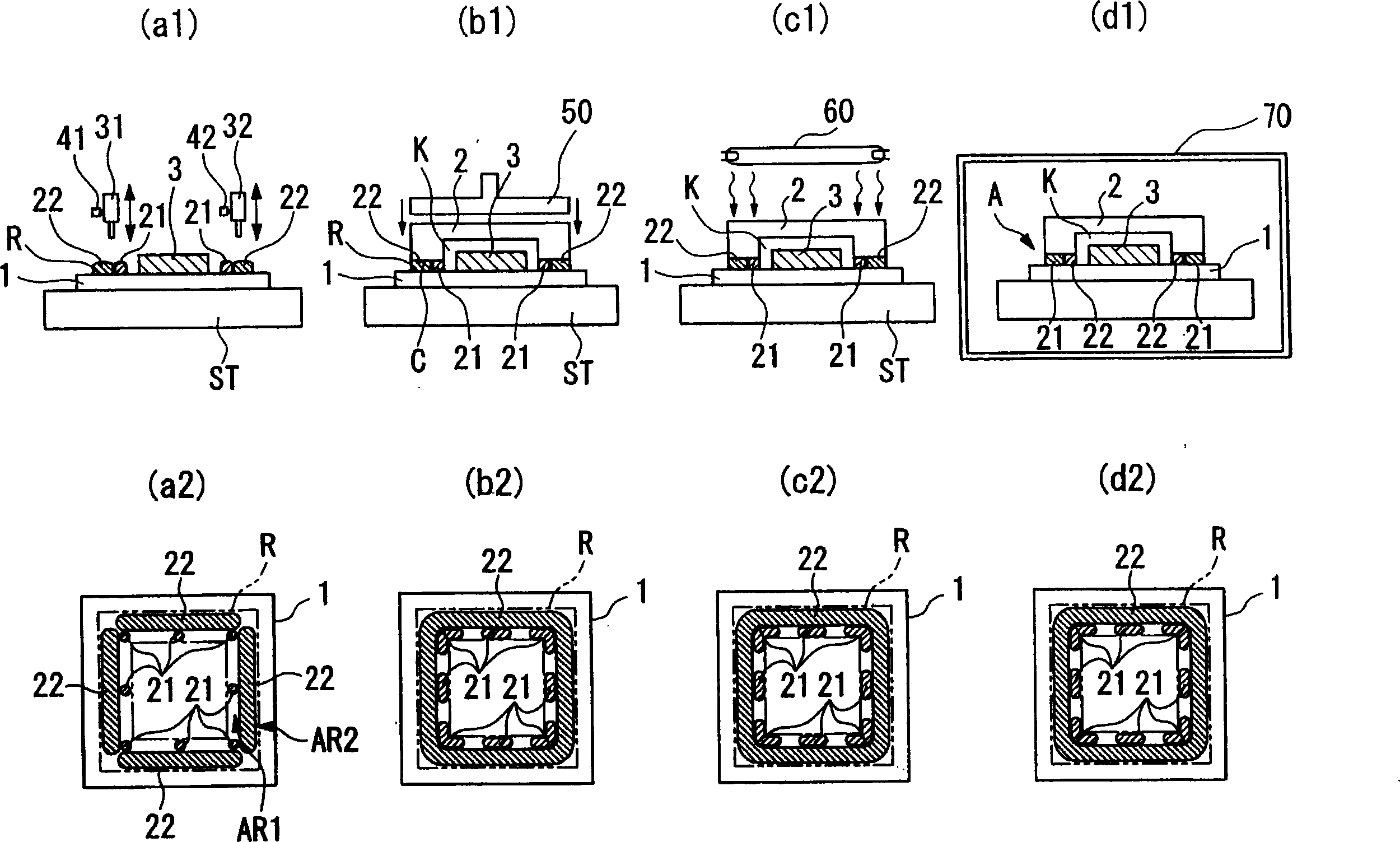
[0084] A first embodiment of the electro-optical device manufacturing method and manufacturing apparatus, the electro-optical device, and the electronic device of the present invention will be described below with reference to the drawings.
[0085] Here, for example, a case where the electro-optical device of the present invention is used as an organic EL device will be described as an example.
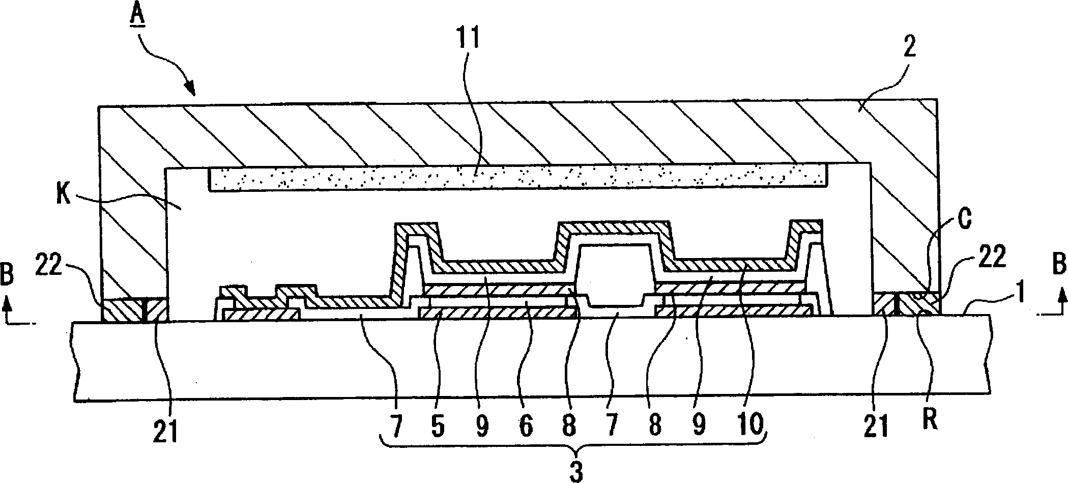
[0086] figure 1 It is a cross-sectional view of an essential part of an organic EL device (electro-optical device). figure 1 The organic EL device (electro-optical device) A includes a substrate (first member) 1, a light-emitting element 3 provided on the substrate 1, and a sealing substrate (second member) 2 as a sealing material bonded to the substrate 1. .
[0087] in figure 1 The organic EL device A shown is an embodiment in which the light emitted by the light-emitting element 3 is taken out from the side of the substrate 1 to the outside of the device. The material for formi...
Embodiment approach 2
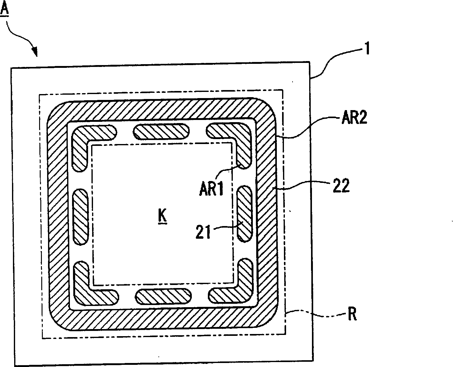
[0146] Figure 7 It is a sectional view of main parts of an organic EL device (electro-optical device) according to a second embodiment of the present invention. Figure 7 Among them, an organic EL device (electro-optical device) A includes a substrate (first member) 1 , a light emitting element 3 provided on the substrate 1 , and a sealing substrate (second member) 2 bonded to the substrate 1 as a sealing member.
[0147] In this example, the substrate 1 and the sealing substrate 2 are bonded together using only the first adhesive 21 (hereinafter simply referred to as the adhesive 21) without the second adhesive 22, which is different from that of the organic EL device according to the first embodiment. different, since the other parts are the same, descriptions about the structure are omitted.
[0148] Figure 8 is along Figure 7 Cross-sectional view of the B-B arrow. Such as Figure 8 As shown, an adhesive 21 is provided on the portion R where the upper surface of the...
Embodiment approach 3
[0205] Hereinafter, an electronic device equipped with the organic EL device A according to Embodiments 1 and 2 will be described as an example.
[0206] Figure 16 (a) is a perspective view showing an example of a portable telephone. Figure 16 In (a), reference numeral 1000 denotes a mobile phone main body, and reference numeral 1001 denotes a display portion using the organic EL device A described above.
[0207] Figure 16 (b) is a perspective view showing a watch-type electronic device. Figure 16 In (b), reference numeral 1100 denotes a portable watch main body, and reference numeral 1101 denotes a display portion using the organic EL device A described above.
[0208] Figure 16 (c) is a perspective view showing an example of a portable information processing device such as a word processor or a personal computer. Figure 16 In (c), reference numeral 1200 denotes an information processing device, reference numeral 1202 denotes an input part such as a keyboard, 1204...
PUM
 Abstract
Description
Claims
Application Information