Motherboard of liquid crystal display

A liquid crystal display, motherboard technology, applied in static indicators, nonlinear optics, optics, etc., can solve problems such as high cost and reduced process time

Active Publication Date: 2007-02-21
AU OPTRONICS CORP
View PDF0 Cites 19 Cited by
  • Summary
  • Abstract
  • Description
  • Claims
  • Application Information

AI Technical Summary

Problems solved by technology

[0005] In view of this, the purpose of the present invention is to provide a liquid crystal display motherboard, which can effectively solve the problem of high cost of traditional PSA technology, and can directly do alignment treatment on the liquid cr...

Method used


Image

  • Motherboard of liquid crystal display
  • Motherboard of liquid crystal display
  • Motherboard of liquid crystal display

Examples


no. 1 example

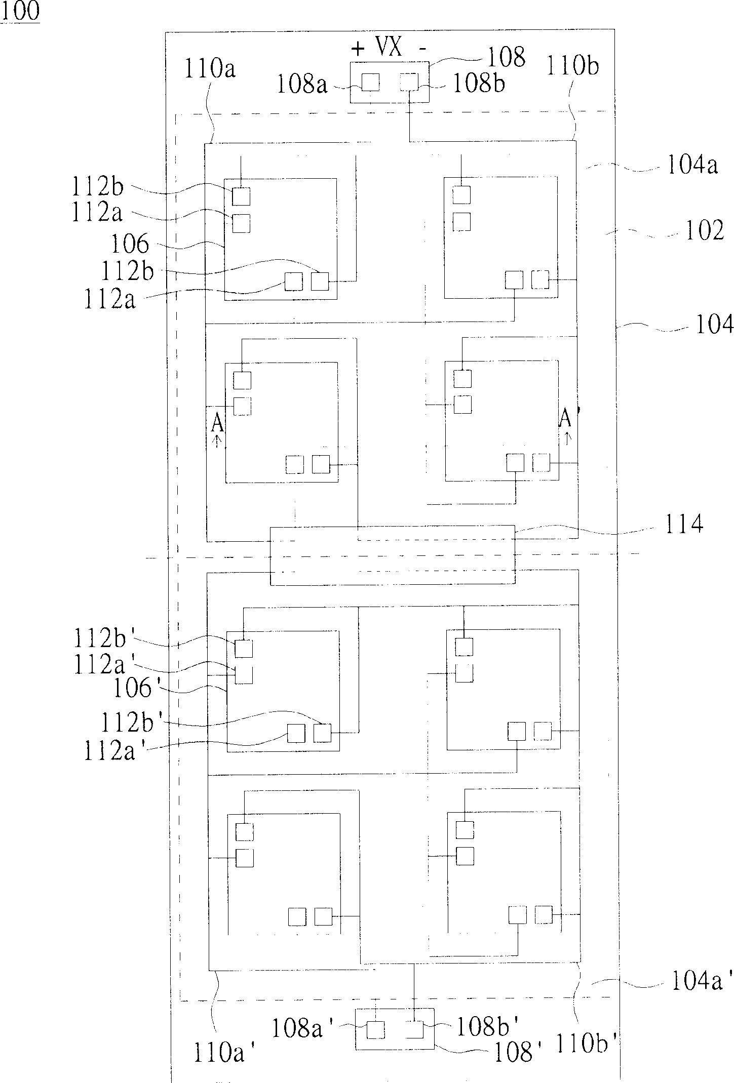
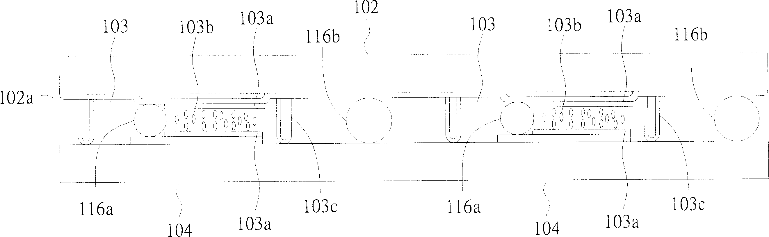
[0043] Please refer to Figure 1A , 1B and 1C, Figure 1A Showing the top structural view of the liquid crystal display motherboard of the first embodiment of the present invention, Figure 1B exhibit Figure 1A The cross-sectional structure diagram of the cross-hatching line formed by A and A', Figure 1C exhibit Figure 1B A detailed top view of the mid-panel area. The liquid crystal display motherboard 100 includes a first substrate 102 , a second substrate 104 and at least one liquid crystal layer 103 . The second substrate 104 is arranged in parallel with the first substrate 102, and the second substrate 104 includes voltage application regions 104a, 104a', input circuits 108, 108', traces 110a, 110b, 110a', 110b' and panel input terminals 112a, 112b, 112a' and 112b'.

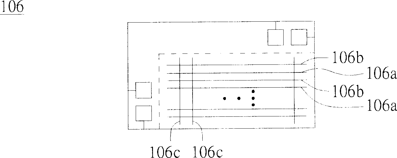
[0044] The voltage application areas 104a and 104a' of the liquid crystal display motherboard 100 of this embodiment have a plurality of panel areas 106 and 106' respectively. The panel regions 106 in...

no. 2 example

[0057] Please refer to figure 2 , which shows a top structural view of a liquid crystal display motherboard according to a second embodiment of the present invention. The difference between this embodiment and the first embodiment is that the liquid crystal display motherboard 200 of this embodiment also has an input circuit 208, a grid panel input terminal 212a, a source panel input terminal 212b, and wires 210a and 210b, and the input circuit 208 includes a gate pad input 208a and a source pad input 208b. The gate and source panel input terminals 212a and 212b of each panel area 106 are electrically connected to the wires 210a and 210b, respectively, and are electrically connected to the scan line and the data line of the panel area, respectively. Gate and source motherboard inputs 208a and 208b are electrically connected to traces 210a and 210b, respectively. That is, the gate panel input terminal 212a is electrically connected to the gate motherboard input terminal 208a...


PUM


Abstract

A mother board of liquid crystal display is prepared as setting liquid crystal layer between the first base plate and the second base plate on region of face plate, setting the first input circuit with the first and the second mother board input ends on each voltage region, setting multiple face plate regions on each voltage region, setting the first and the second wirings on each voltage region and electric-connecting them separately to the first and the second mother board input ends, setting the first and the second face plate ends on each face plate region and electric-connecting them to the first and the second wirings.

Description

technical field [0001] The present invention relates to a liquid crystal display motherboard (sheet), in particular to a liquid crystal display motherboard capable of simultaneously performing polymer stabilization alignment (Polymer Stabilization Alignment, PSA) technology on each liquid crystal display panel therein. Background technique [0002] In today's era of rapid technological development, liquid crystal display panels have been widely used in electronic display products, such as televisions, computer screens, notebook computers, mobile phones or personal digital assistants. In particular, the multi-domain alignment liquid crystal display panel prepared by polymer-stabilized alignment (PSA) technology has fast response time, wide viewing angle, high aperture ratio, and high contrast. And the advantages of simple manufacturing process, etc., have always been a technology that has been valued by the industry. [0003] In the PSA technology, in the process of preparin...

Claims


Application Information

Patent Timeline
IPC IPC(8): G02F1/133G09G3/36G02F1/1339
Inventor 董人郎陈雅洁
Owner AU OPTRONICS CORP
Why Eureka
Try Eureka