RF circuit with stacked printed circuit boards
A technology of substrate and conductive interconnection, applied in the field of RF circuits, can solve the problems of limited design and manufacturing costs, small space, and having to be replaced, and achieve good effects of mechanical shock and vibration
- Summary
- Abstract
- Description
- Claims
- Application Information
AI Technical Summary
Problems solved by technology
Method used
Image

Examples
Embodiment Construction
[0026] Throughout the drawings, schematic representations of components and substrates are shown. These components are for illustrative purposes only and do not limit the scope of the present invention.
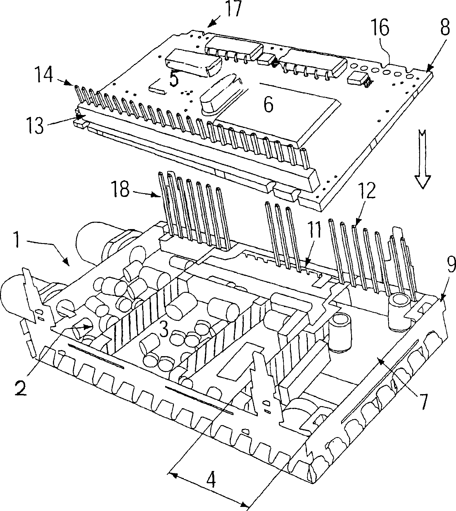
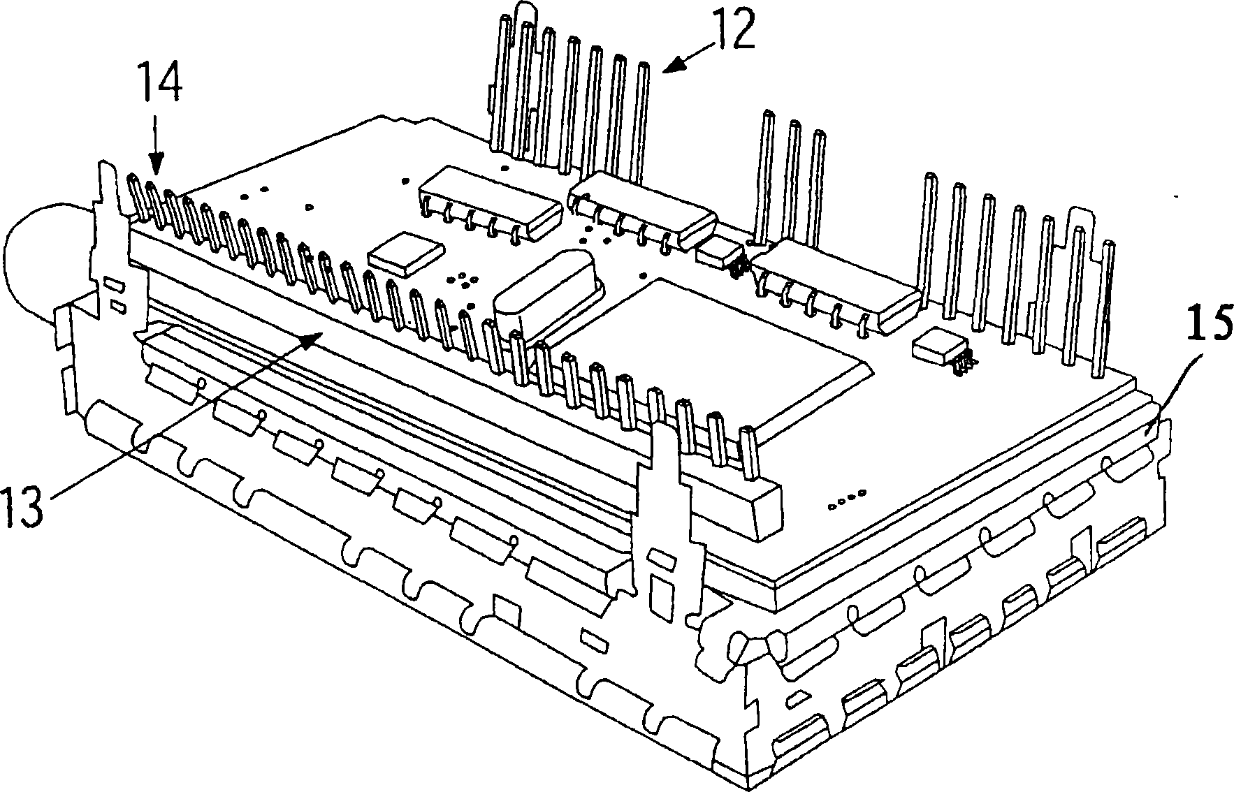
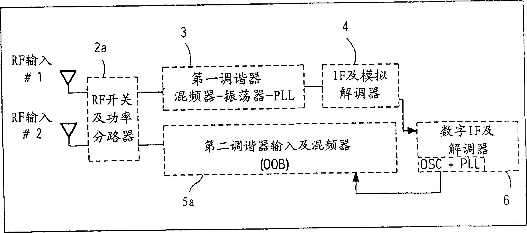
[0027] figure 1 An exploded perspective view of an embodiment of an RF unit according to the invention is shown. The RF unit as a whole is identified with reference number 1 . The RF unit 1 comprises, an RF switch and an RF splitter or circulator 2 , a first tuner 3 and an IF and analog demodulator 4 on a first substrate 7 . A second tuner or remodulator 5 and a demodulator 6 are arranged on a second substrate 8 . The first substrate 7 is mounted on figure 1 In the upper part of the housing 9, it is preferably made of sheet metal to shield against electromagnetic radiation. exist figure 1 In , the housing 9 is shown inverted. In a preferred embodiment, the housing 9 is made from a piece of metal which is cut and bent to form a rectangular tube with one or two open majo...
PUM
 Abstract
Description
Claims
Application Information
 - R&D Engineer
- R&D Manager
- IP Professional
- Industry Leading Data Capabilities
- Powerful AI technology
- Patent DNA Extraction
Browse by: Latest US Patents, China's latest patents, Technical Efficacy Thesaurus, Application Domain, Technology Topic.
© 2024 PatSnap. All rights reserved.Legal|Privacy policy|Modern Slavery Act Transparency Statement|Sitemap