Packaging structure for optical sensing assembly and method of manufacture

A technology of packaging structure and manufacturing method, which is applied in semiconductor/solid-state device manufacturing, electrical components, electric solid-state devices, etc., and can solve problems such as difficult to remove pollutants and affect the function of light-sensing chip 20

Inactive Publication Date: 2007-02-28
SIGURD MICROELECTRONICS CORP
View PDF0 Cites 10 Cited by
  • Summary
  • Abstract
  • Description
  • Claims
  • Application Information

AI Technical Summary

Problems solved by technology

However, when the space (S2) between the photo-sensing chip 20 and the frame 14 is too small, it will be difficult to remove the pollutants during cleaning. In other words, the pollutants between the photo-sensing chip 20 and the frame 14 are not easily removed. Clean up and affect the function of the light sensing chip 20

Method used


Image

  • Packaging structure for optical sensing assembly and method of manufacture
  • Packaging structure for optical sensing assembly and method of manufacture
  • Packaging structure for optical sensing assembly and method of manufacture

Examples


Embodiment Construction

[0042] In the following, specific embodiments are described in detail with reference to the accompanying drawings, so that it is easier to understand the purpose, technical content, features and effects of the present invention.

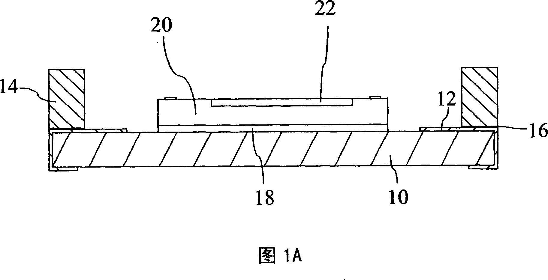
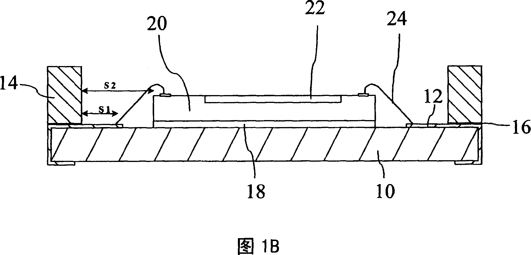
[0043] The invention relates to a packaging structure of a photo-sensing component and a manufacturing method of the packaging structure, which provide a mechanism for light to penetrate into the photo-sensing component and protect the photo-sensing chip inside from being polluted by external particles.

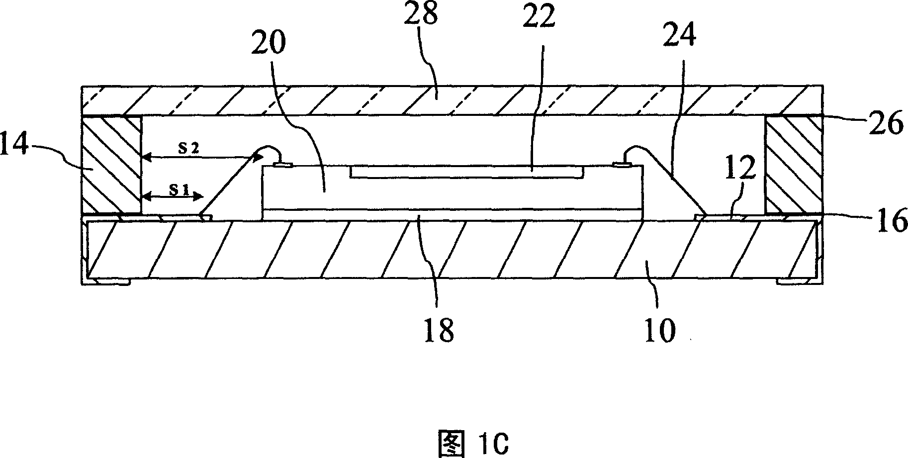
[0044] The basic structure of the new optical sensor package structure of the present invention is shown in FIG. Adhesive on the substrate 30, the photo-sensing chip 34 has a photo-sensing area (Sensor Area) 38, the electrical communication between the photo-sensing chip 34 and the substrate 30 is connected by metal wires (Bond wires) 40, and there is a A Light transparent cover lid 42 has a cavity design, so that the cover 42 is bonded to the subst...


PUM


Abstract

The invention relates to a package of light-sensitive element and relative production. Wherein, it comprises: mounting light-sensitive chip on the base plate; clearing the contaminant; then using adhesive to mount a transparent sealing cover with chamber above the base plate, to cover the chip; therefore, it can clear the contaminant, improve the yield and reduce the packing area; in addition, the invention can arrange connecting part above the base plate and sealing cover to support connection.

Description

technical field [0001] The present invention relates to a packaging technology of a photo-sensing component, in particular to a packaging structure of a photo-sensing component capable of protecting a photo-sensing chip from being polluted by external particles and a manufacturing method thereof. Background technique [0002] Press, CMOS photo-sensing component is a kind of photo-sensing component manufactured using photoelectric related technology principles, which can be widely used in imaging products such as security monitoring, digital cameras, toys, mobile phones, PDAs, video phones, fingerprint readers, etc. [0003] Please refer to FIG. 1A to FIG. 1C for the packaging methods of the known CMOS photo-sensing components. First, as shown in FIG. 1A, a substrate 10 with a metal wiring layer 12 is provided, and a frame (Frame) 14 is adhered around the substrate 10 by a first glue layer (Glue Layer) 16, and then an adhesive 18 is used to attach the photosensitive The dete...

Claims


Application Information

Patent Timeline
Patent Type & Authority Applications(China)
IPC IPC(8): H01L27/14H01L21/50H01L31/0203
CPCH01L2224/48091H01L2224/73265H01L2924/16152H01L2924/16195
Inventor 陈柏宏
Owner SIGURD MICROELECTRONICS CORP
Why Eureka
Try Eureka