
Light emitting diode package and method for manufacturing the same

A technology for light-emitting diodes and packages, applied in semiconductor devices, electrical components, circuits, etc., can solve the problems of deteriorating phosphors, reducing light extraction efficiency, and deteriorating thermal characteristics, preventing the reduction of light extraction efficiency and enhancing uniform light emission. characteristics, the effect of reducing the optical path difference

Inactive Publication Date: 2007-03-28
SAMSUNG ELECTRO MECHANICS CO LTD
View PDF0 Cites 12 Cited by
  • Summary
  • Abstract
  • Description
  • Claims
  • Application Information

AI Technical Summary

Problems solved by technology

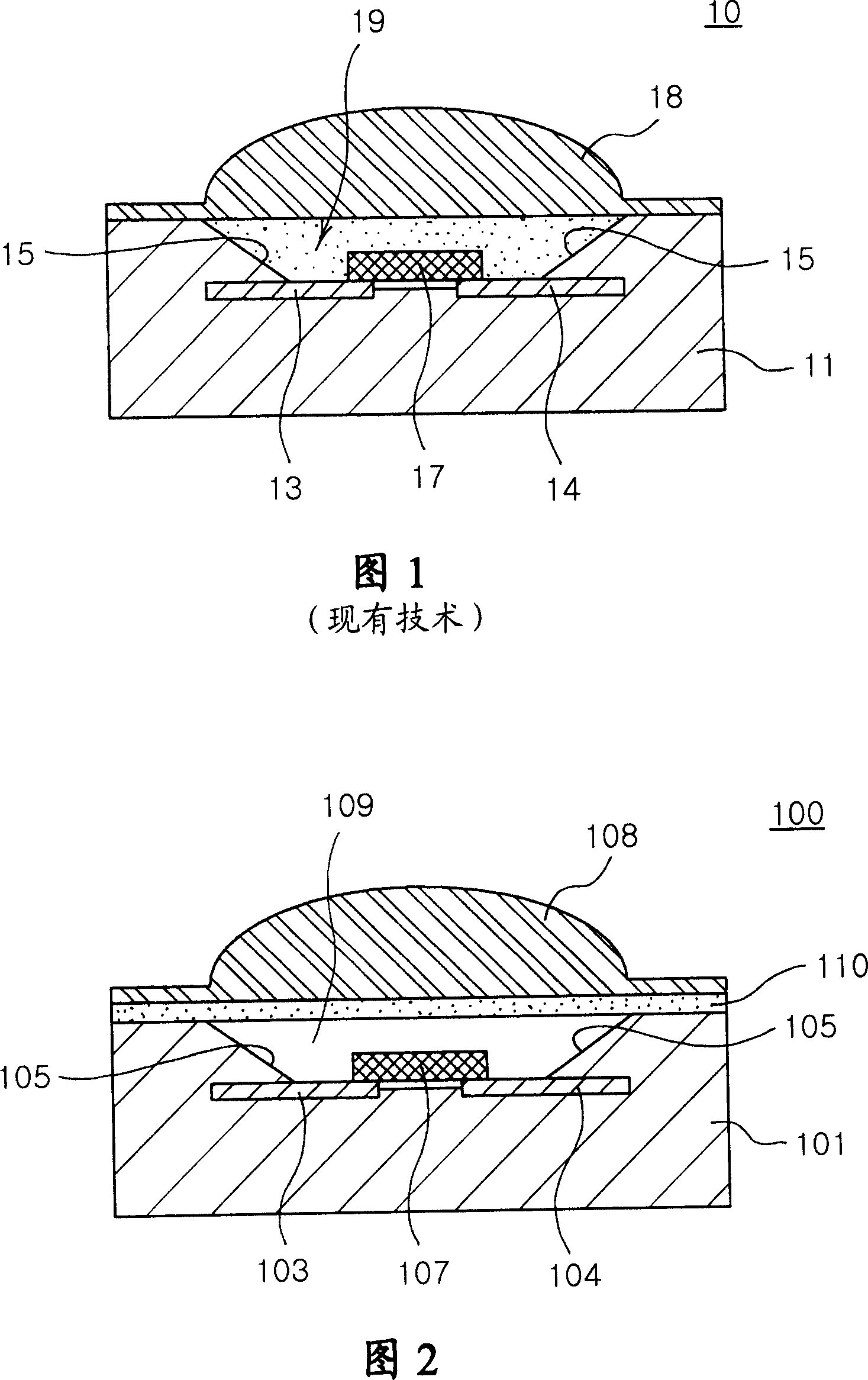
According to this conventional LED package 10, since the LED chip 17 is in direct contact with the resin, the heat generated from the LED chip 17 is directly transferred to the resin, thereby easily deteriorating the resin and the phosphor.
This may make it impossible to obtain the desired wavelength of light
In fact, the resin has a very low thermal conductivity of 0.2 ~ 1W / m.K, so the heat generated from the LED chip is not easily released, thereby deteriorating the phosphor powder dispersed in the resin
Therefore, the light extraction efficiency is lowered and uniform light emission is hindered due to deterioration of the thermal characteristics of the phosphor-containing resin.

Method used


Image

  • Light emitting diode package and method for manufacturing the same
  • Light emitting diode package and method for manufacturing the same
  • Light emitting diode package and method for manufacturing the same

Examples


Embodiment Construction

[0028] The present invention will now be described more fully with reference to the accompanying drawings, in which preferred embodiments of the invention are shown. However, this invention may be embodied in many different forms and should not be construed as limited to the embodiments described herein. Rather, these embodiments are provided so that those skilled in the art will fully disclose and fully cover the scope of the present invention. In the drawings, the size and relative sizes of layers and regions may be exaggerated for clarity, and the same reference numerals will be used herein to designate the same or like components.

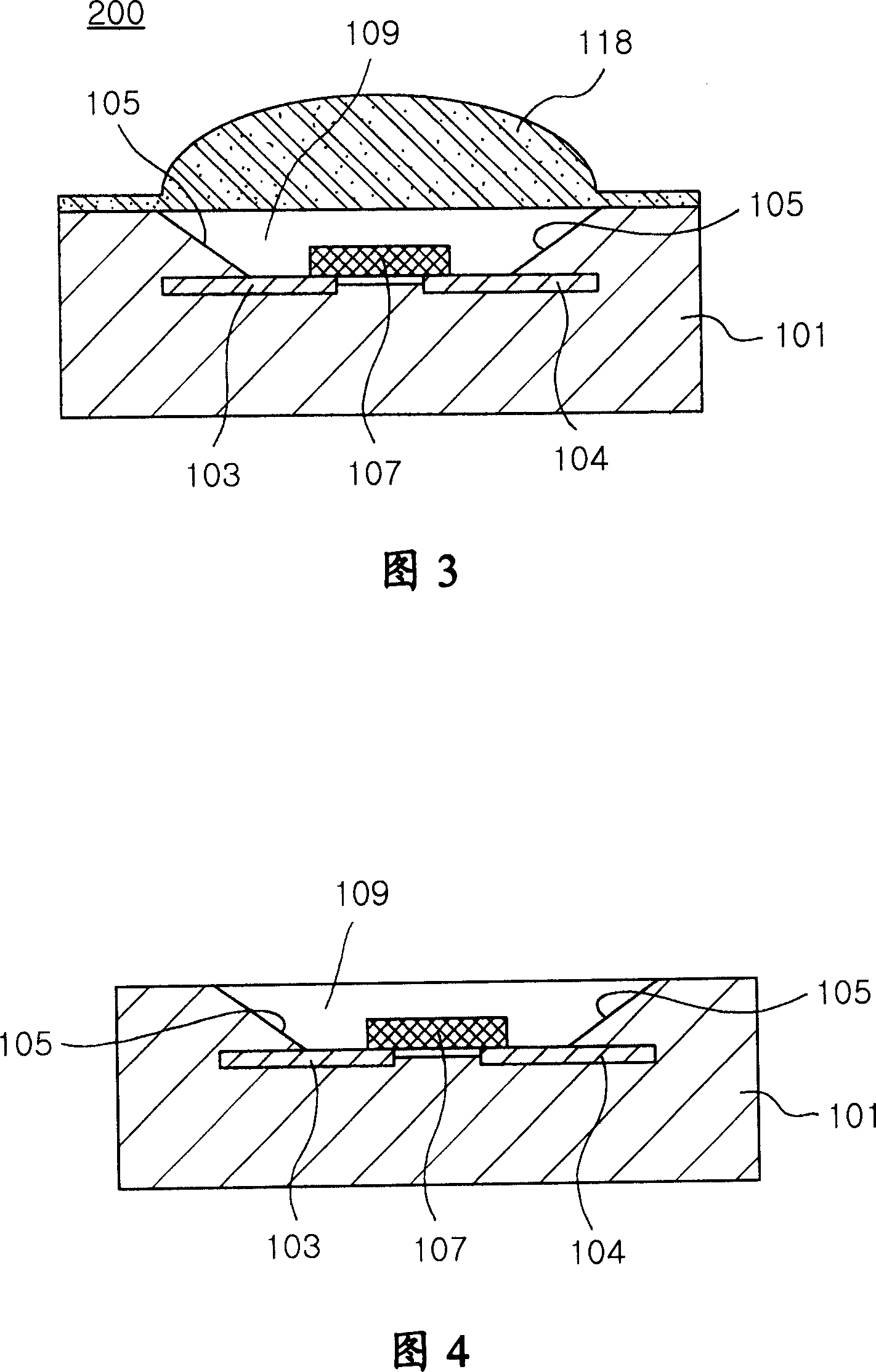
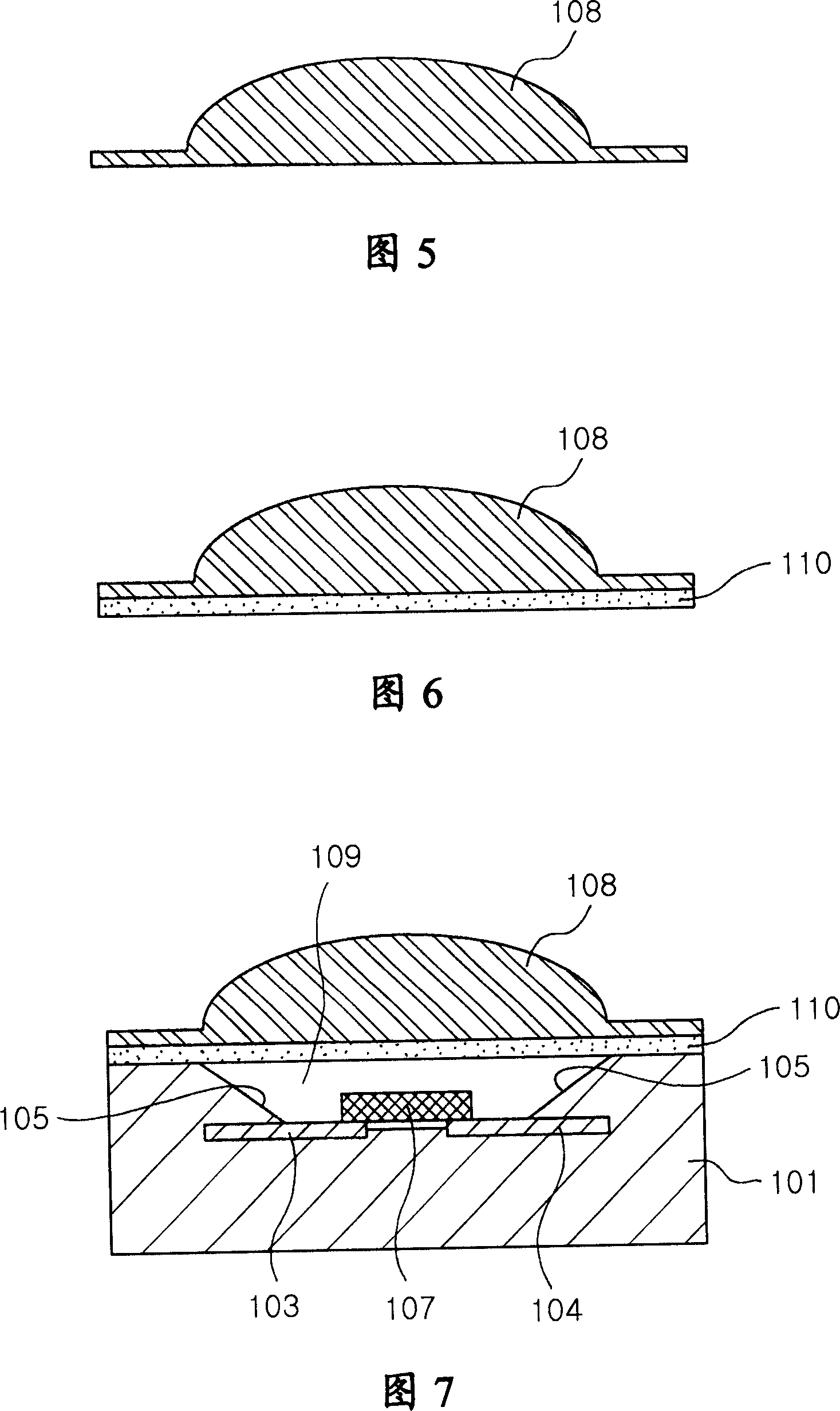
[0029] FIG. 2 is a side sectional view showing an LED package 100 according to an embodiment of the present invention. Referring to FIG. 2 , the LED package 100 includes a package body 101 having a recess 109 and an LED chip 107 mounted on the package body 101 . The package body 101 may be made of polymer or ceramic. The lead electrodes 103 ...


PUM


Abstract

The invention relates to a light emitting diode package that can prevent deterioration of phosphor and a method of manufacturing the same. The light emitting diode package includes a package body having a recessed part, a light emitting diode chip mounted on a floor surface of the recessed part and a lens structure disposed on an upper surface of the package body, apart from the light emitting diode chip. Phosphor is dispersed in at least a part of the lens structure.

Description

[0001] priority statement [0002] This application claims priority from Korean Patent Application No. 2005-88338 filed with the Korean Intellectual Property Office on September 22, 2005, the disclosure of which is incorporated herein by reference. technical field [0003] The present invention relates to a light emitting diode package and a manufacturing method thereof, and more particularly, to a light emitting diode package capable of preventing phosphors from being degraded so as to have high light extraction efficiency and a manufacturing method thereof. Background technique [0004] In recent years, light emitting diodes (hereinafter, referred to as 'LEDs') have been used as light sources of various colors. In particular, with the increasing demand for high-output, high-brightness LEDs such as white LEDs for lighting, methods for enhancing the capability and reliability of LED packages have been actively researched. In general, excellent performance of LED products is...

Claims


Application Information

Patent Timeline
Patent Type & Authority Applications(China)
IPC IPC(8): H01L33/00H01L33/44H01L33/50H01L33/56H01L33/58
CPCH01L33/507H01L33/58
Inventor 金勇植崔硕文林昶贤金容锡
Owner SAMSUNG ELECTRO MECHANICS CO LTD
Learn More