Device and method for joining substrates

A substrate and sealing substrate technology, applied in the direction of semiconductor/solid-state device components, semiconductor devices, electrical components, etc., to achieve the effect of improving efficiency and preventing contamination

Inactive Publication Date: 2007-03-28
FUJIFILM CORP
View PDF3 Cites 16 Cited by
  • Summary
  • Abstract
  • Description
  • Claims
  • Application Information

AI Technical Summary

Problems solved by technology

However, WLCSP-type solid-state imaging devices using opaque materials as spacers cannot use laser displacement meters for parallelism measurement
Note that the documents of Japanese Patent Laid-Open Nos. 2002-329850, 2003-163342, and Japanese Patent Application No. 2003-320271 do not propose a solution to the problems occurring in bonded substrates

Method used


Image

  • Device and method for joining substrates
  • Device and method for joining substrates
  • Device and method for joining substrates

Examples


Embodiment Construction

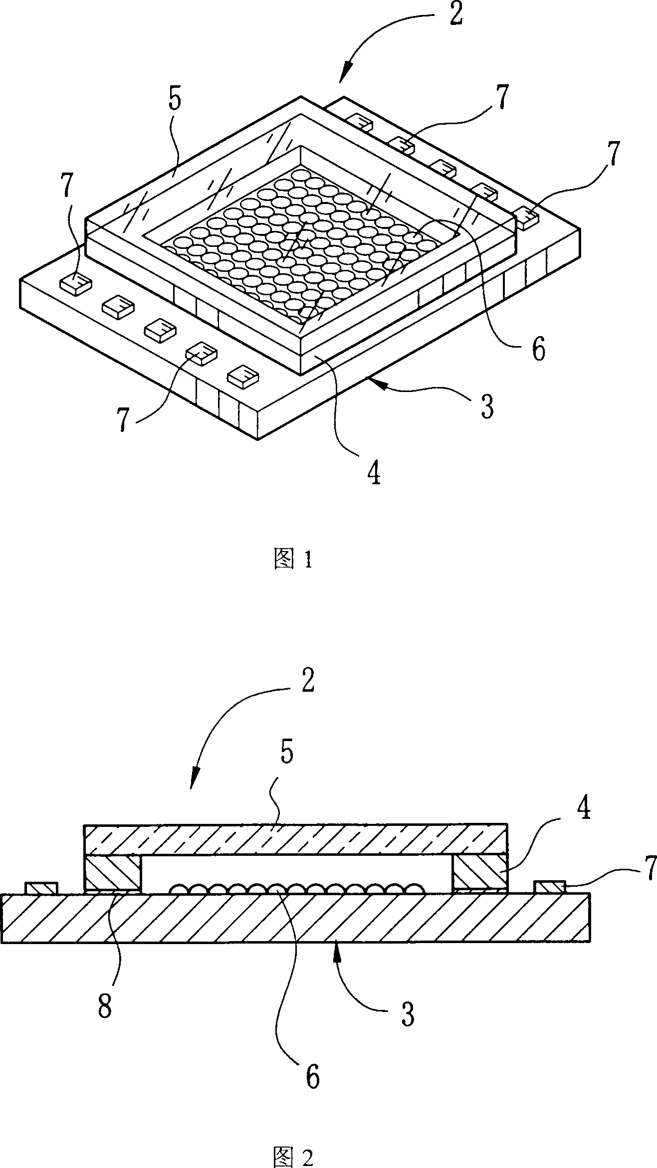
[0068] As shown in FIGS. 1 and 2, a WLCSP type solid-state imaging device 2 consists of an image sensor chip 3, a frame-shaped spacer 4 bonded to the image sensor chip 3 by an adhesive 8, and a frame-shaped spacer 4 bonded to the spacer 4 for The protective glass 5 that seals the interior of the spacer 4 constitutes.

[0069] On the image sensor chip 3 , there are an image sensor 6 including a plurality of pixels and a plurality of contact terminals 7 electrically connected to the image sensor 6 . The plurality of pixels generate electrical signals according to the amount of light received. For example, the image sensor 6 is a CCD (Charge Coupled Device) on which color filters and microlenses are superimposed. The contact terminals 7 are for printing conductive material on eg the image sensor chip 3 . In the same manner, each contact terminal 7 is connected with the image sensor 6 through printed wiring.

[0070] The spacer 4 is made of an inorganic material such as silicon...


PUM


Abstract

A device for joining substrates (11) is provided inside a clean booth (12). a single axis robot (46) and a five axis robot (47) convey a wafer (25) and a glass substrate (33). A transcribing station (91) obtains a transcribing film (112) on which adhesive is applied from a film supplying section (113), and presses the transcribing film (112) to the glass substrate (33) so as to transcribe the adhesive to the glass substrate (33). A peeling station (92) peels the transcribing film (112) from the glass substrate (33). A joining station (57) positions the wafer (25) and the glass substrate (33), adjusts parallelism of joining surfaces of the wafer (25) and the glass substrate (33), and joins these substrates together. Since the handling and the joining of the wafer (25), the glass substrate (33) and the transcribing film (112) are performed in the clean booth, it is prevented that a yield ratio of the product decreases because of the adhesion of foreign matters.

Description

technical field [0001] The present invention relates to an apparatus and method for bonding semiconductor substrates and sealing substrates in the manufacture of chip-sized packages. Background technique [0002] Digital cameras and digital video cameras having solid-state imaging devices such as CCDs and CMOSs ​​are widely used. A semiconductor substrate in a conventional solid-state imaging device, that is, an image sensor chip, is contained in a package and sealed by transparent glass ribs. However, solid-state imaging devices are required to be downsized due to an increase in demand for mobile phones having a function of carrying images and the like. [0003] Wafer level chip size packaging (hereinafter referred to as WLCSP) is a packaging method for downsizing a solid-state imaging device. In the semiconductor wafer process, when the packaging is completed, the semiconductor devices in the WLCSP are obtained by dicing the wafer by scribing. A solid-state imaging devi...

Claims


Application Information

Patent Timeline
Patent Type & Authority Applications(China)
IPC IPC(8): H01L23/02H01L27/14
Inventor 高﨑康介山本清文奥津和雄辻村幸治
Owner FUJIFILM CORP
Why Eureka
Try Eureka