
Optical member, method of manufacturing the optical member, and display device having the optical member

A technology for optical components and display devices, which is applied in the field of optical components, can solve problems such as increased costs, and achieve the effect of reducing costs

Inactive Publication Date: 2007-04-04
SAMSUNG ELECTRONICS CO LTD
View PDF0 Cites 6 Cited by
  • Summary
  • Abstract
  • Description
  • Claims
  • Application Information

AI Technical Summary

Problems solved by technology

However, the additional optical flakes lead to increased cost in the manufacture of the backlight assembly

Method used


Image

  • Optical member, method of manufacturing the optical member, and display device having the optical member
  • Optical member, method of manufacturing the optical member, and display device having the optical member
  • Optical member, method of manufacturing the optical member, and display device having the optical member

Examples


Embodiment Construction

[0028] The invention will be described more fully hereinafter with reference to the accompanying drawings, in which embodiments are shown. However, the present invention can be implemented in various forms and is not limited to the following examples. Rather, these embodiments are provided so that this disclosure will be thorough and complete, and will fully convey the scope of the invention to those skilled in the art, and in the figures, the dimensions of layers and regions and relative dimensions may be exaggerated for clarity.

[0029] It can be understood that when an element or layer is referred to as being located on, connected to, or coupled to another element or layer, it can be directly located on, connected to, or coupled to another element or layer. In turn, intervening elements or layers may also be present. In contrast, when an element is referred to as being directly on, directly connected to or directly coupled to another element or layer, there are no interve...


PUM

PropertyMeasurementUnit
diameteraaaaaaaaaa

Abstract

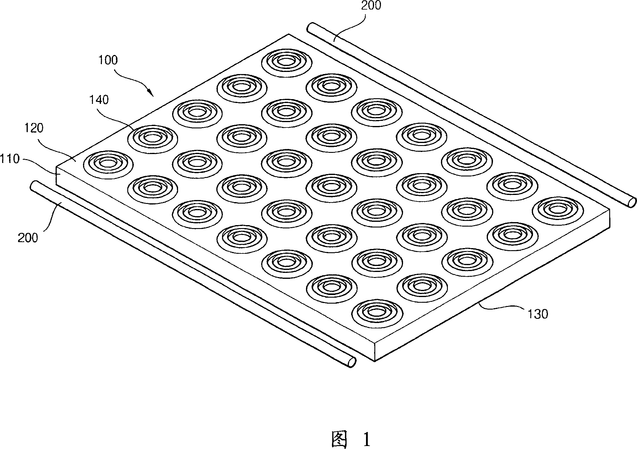
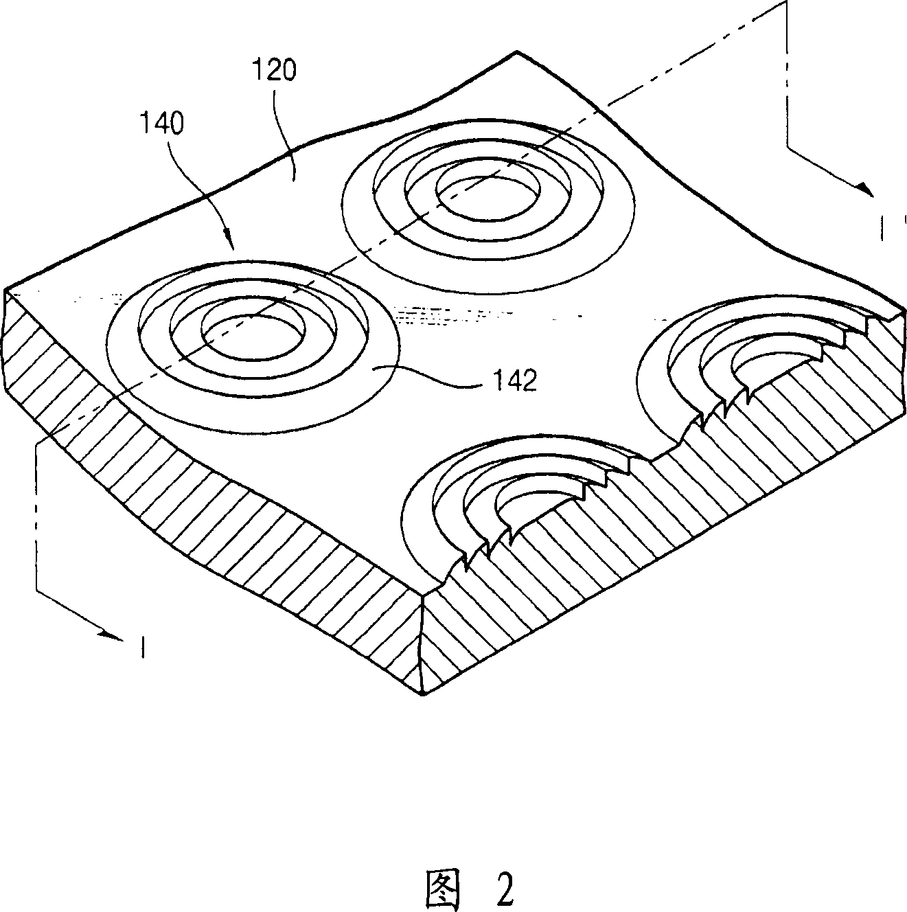
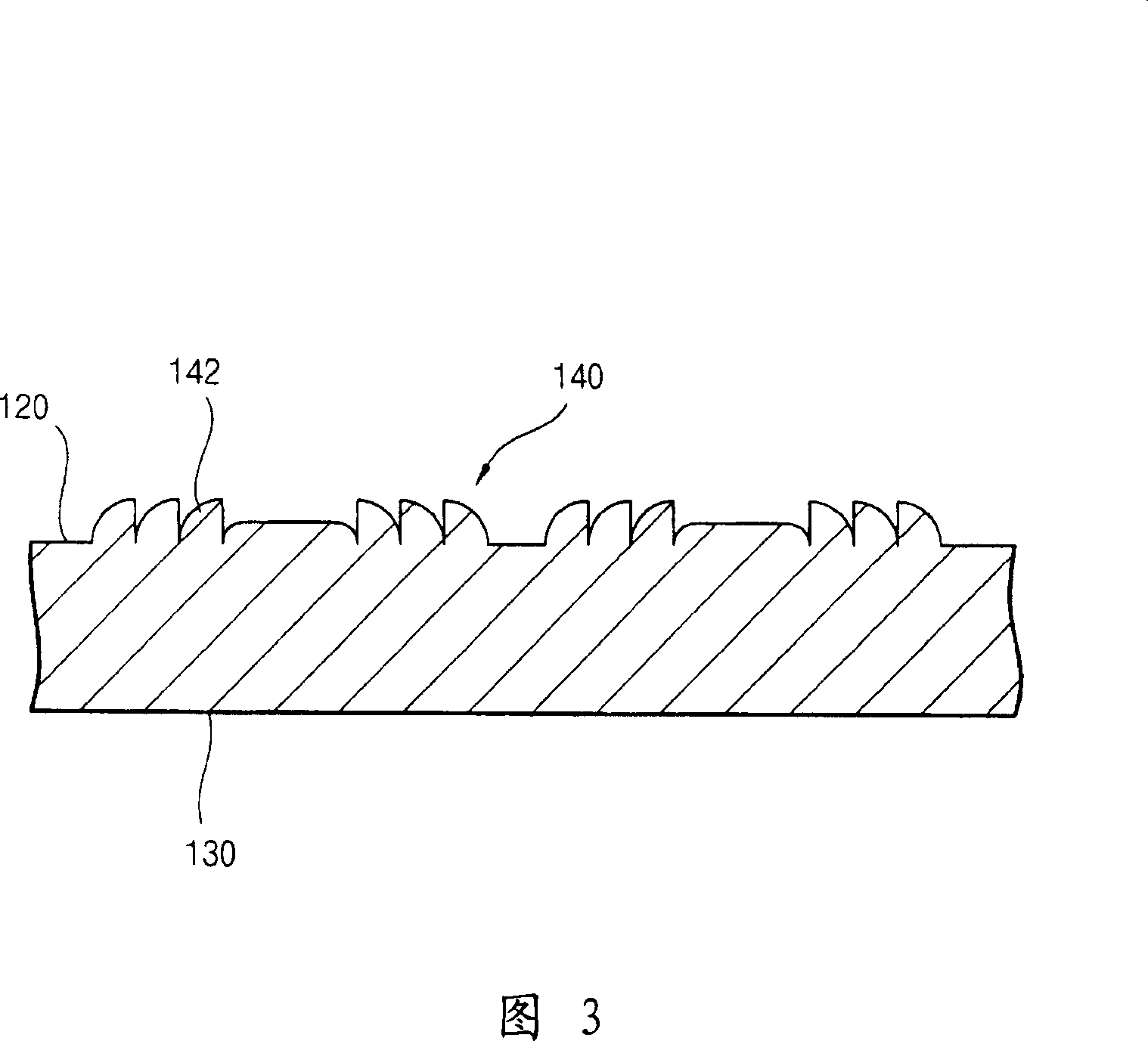
An optical member that lends itself to be more cost-effectively manufactured than a conventional optical member is presented. A display device made with the optical member can be thinner than the conventional optical member. The optical member includes a light-incident face that receives light emitted from a lamp positioned at a side of the optical member, a light-exiting face that is in a plane perpendicular to the light-incident face, and a light reflecting face opposite to the light-exiting face. A light-concentrating pattern having a plurality of concentric circles is formed on the light-exiting face. The light-concentrating pattern may be the Fresnel lens pattern. A diffusing pattern for diffusing the light is formed on the light reflecting face. Since patterns are formed on the optical member, additional optical sheet such as a prism sheet, a reflective polarizing sheet, a diffusion sheet, etc., is unnecessary.

Description

technical field [0001] The present invention relates to an optical element used in a display device, especially an optical element having higher cost efficiency than conventional optical elements. Background technique [0002] Generally, display devices for displaying images are used in information processing equipment such as notebook computers and televisions. Examples of the display device include a cathode ray tube (CRT), a plasma display panel (PDP), a liquid crystal display (LCD), and the like. Among different types of display devices, LCD devices using liquid crystal (LC) molecules to display images are increasingly widely used. [0003] LCD devices display images using liquid crystal molecules with specific optical and electrical properties, such as anisotropic refractive index, anisotropic dielectric constant, and other characteristics. Accordingly, LCDs have advantages such as thinness, lightness, low driving voltage, and low power consumption over other display ...

Claims


Application Information

Patent Timeline
Patent Type & Authority Applications(China)
IPC IPC(8): G02B5/00G02B5/02G02B3/00G02F1/1335
CPCG02F1/133606G02B6/005G02B6/0036G02F1/1335
Inventor 崔震成白晶旭朴辰赫朱炳润河周和
Owner SAMSUNG ELECTRONICS CO LTD
Learn More