Gallium nitride based semiconductor light emitting diode and method of manufacturing the same
A technology of light-emitting diodes and nitride semiconductors, applied in semiconductor devices, electrical components, circuits, etc.
- Summary
- Abstract
- Description
- Claims
- Application Information
AI Technical Summary
Problems solved by technology
Method used
Image
Examples
Embodiment 1
[0048] Structure of GaN-based semiconductor LED
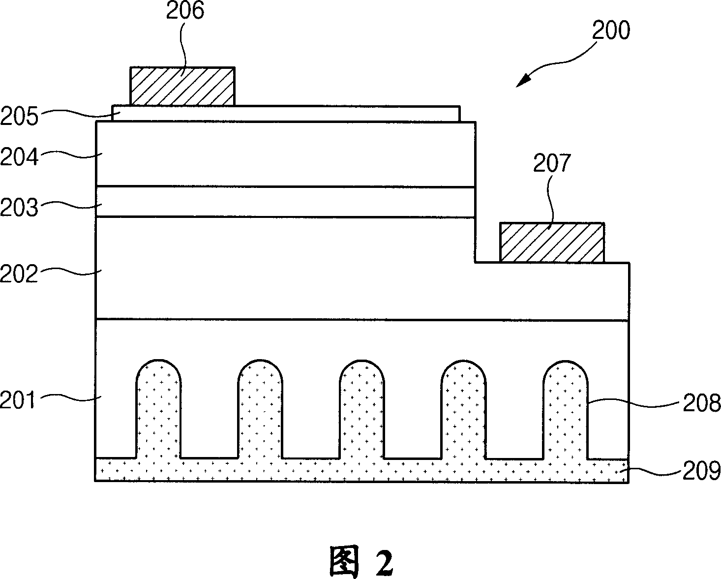
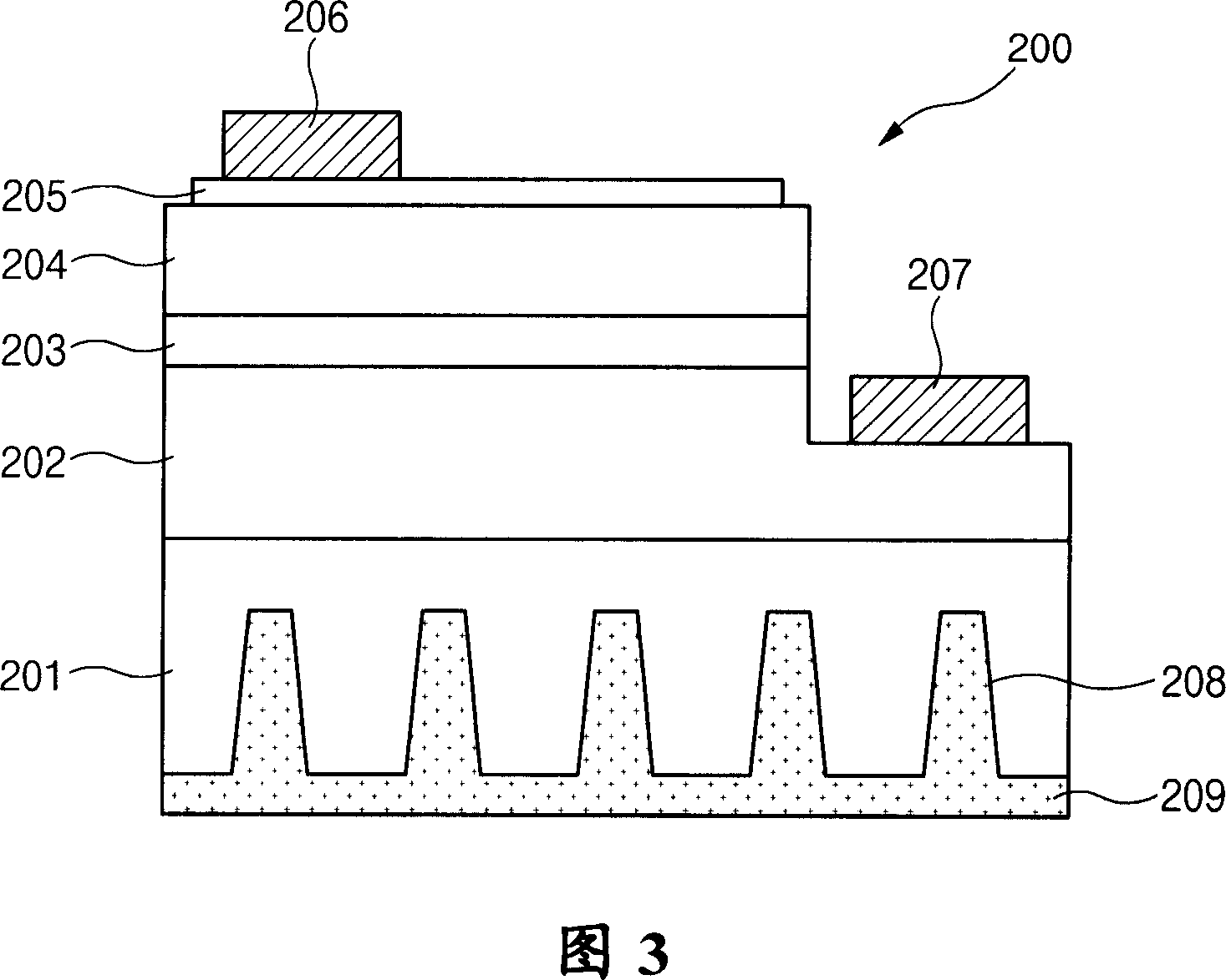
[0049] Next, a GaN-based semiconductor LED according to a first embodiment of the present invention will be described in detail with reference to FIGS. 2 and 3 .
[0050] 2 and 3 are cross-sectional views of a GaN-based semiconductor LED according to a first embodiment of the present invention.
[0051] Referring to FIG. 2 , a GaN-based semiconductor LED 200 includes an n-type nitride semiconductor layer 202 , an active layer 203 , and a p-type nitride semiconductor layer 204 , which are sequentially formed on a sapphire substrate 201 . The sapphire substrate 201 is used to grow GaN-based semiconductor material. A portion of the p-type nitride semiconductor layer 204 and a portion of the active layer 203 are removed by a mesa etching process, thereby exposing a predetermined upper portion of the n-type nitride semiconductor layer 202 .
[0052] The n-type nitride semiconductor layer 202, the p-type nitride semiconductor layer...
Embodiment 2
[0073] Structure of GaN-based semiconductor LED
[0074] Next, a GaN-based semiconductor LED according to a second embodiment of the present invention will be described in detail with reference to FIG. 5 . For brevity, descriptions of the same parts as those of the first embodiment of the present invention will be omitted.
[0075] 5 is a cross-sectional view of a GaN-based semiconductor LED according to a second embodiment of the present invention.
[0076] Referring to FIG. 5, a GaN-based semiconductor LED 300 according to a second embodiment of the present invention has the same structure as the GaN-based semiconductor LED 200 according to the first embodiment of the present invention, except that a substituting heat conduction layer 209 is formed on a lower portion of a sapphire substrate 301. reflective layer 309 to fill the groove 308 outside.
[0077] That is, the GaN-based semiconductor LED 300 according to the second embodiment of the present invention includes: an n-...
Embodiment 3
[0086] Structure of GaN-based semiconductor LED
[0087] Hereinafter, a GaN-based semiconductor LED according to a third embodiment of the present invention will be described in detail with reference to FIG. 6 . For brevity, descriptions of the same parts as those of the first embodiment of the present invention will be omitted.
[0088] 6 is a cross-sectional view of a GaN-based semiconductor LED according to a third embodiment of the present invention.
[0089] Referring to FIG. 6, a GaN-based semiconductor LED 400 according to a third embodiment of the present invention has the same structure as the GaN-based semiconductor LED 200 according to the first embodiment of the present invention, except that a reflective layer 409 whose reflectivity is higher than that of a sapphire substrate 401 is further Formed between a sapphire substrate 401 having a groove 408 and a heat conduction layer 410 .
[0090] That is, the GaN-based semiconductor LED 400 according to the third emb...
PUM
| Property | Measurement | Unit |
|---|---|---|
| diameter | aaaaa | aaaaa |
Abstract
Description
Claims
Application Information
 - R&D Engineer
- R&D Manager
- IP Professional
- Industry Leading Data Capabilities
- Powerful AI technology
- Patent DNA Extraction
Browse by: Latest US Patents, China's latest patents, Technical Efficacy Thesaurus, Application Domain, Technology Topic, Popular Technical Reports.
© 2024 PatSnap. All rights reserved.Legal|Privacy policy|Modern Slavery Act Transparency Statement|Sitemap|About US| Contact US: help@patsnap.com


