Lead frame for semiconductor device and manufacturing methode thereof

A lead frame and manufacturing method technology, applied in semiconductor/solid-state device manufacturing, semiconductor devices, semiconductor/solid-state device components, etc., can solve the problems of increasing the cost of semiconductor devices and high cost ratio, and achieve faster response and lower overall Price, the effect of reducing deterioration

Inactive Publication Date: 2007-04-18
开益禧有限公司
View PDF0 Cites 4 Cited by
  • Summary
  • Abstract
  • Description
  • Claims
  • Application Information

AI Technical Summary

Problems solved by technology

[0009] Second, even if the specified metal satisfies the above-mentioned various material properties, its price should not be higher than that of the previous lead frame (for example: 42 alloy)
For example, when a lead frame made of a 42 alloy is used in a semiconductor device, the lead frame made of the 42 alloy accounts for a very high proportion of the cost of the semiconductor device, resulting in an increase in the cost of the semiconductor device itself

Method used


Image

  • Lead frame for semiconductor device and manufacturing methode thereof
  • Lead frame for semiconductor device and manufacturing methode thereof
  • Lead frame for semiconductor device and manufacturing methode thereof

Examples


Embodiment Construction

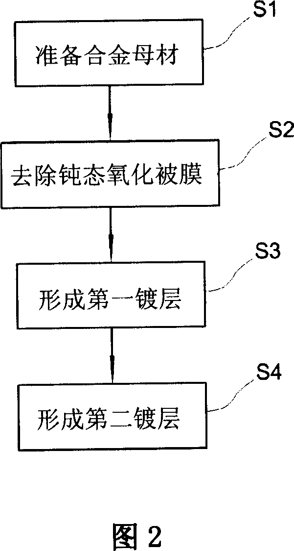
[0030] Hereinafter, the present invention will be described in detail with reference to the drawings.

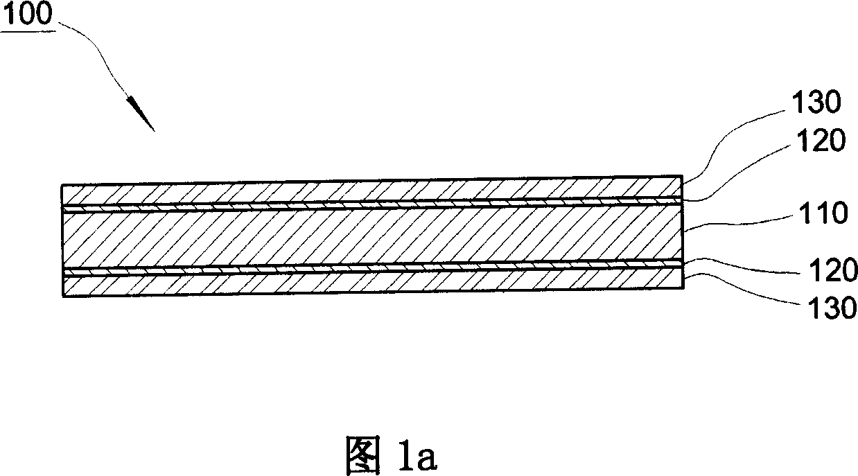
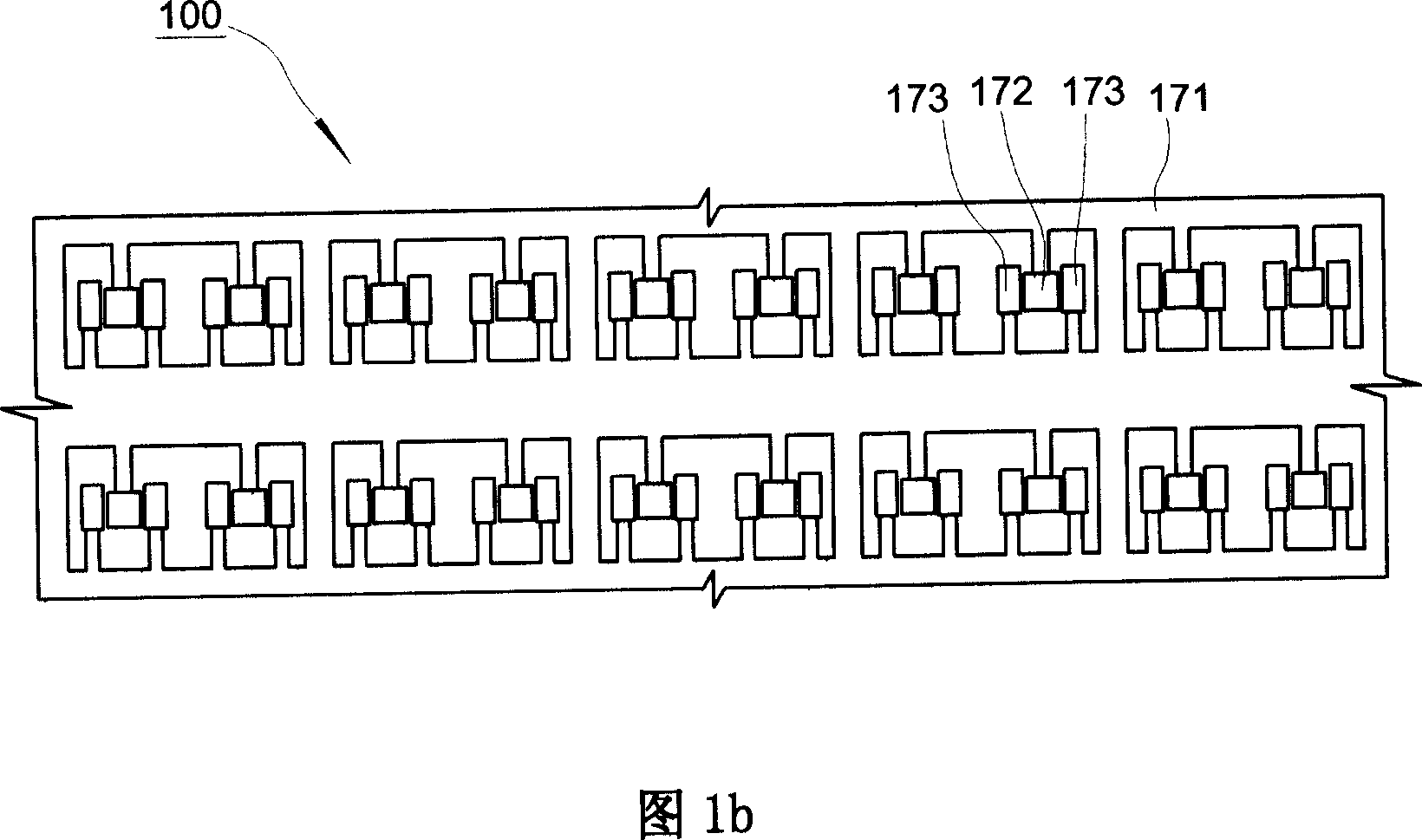
[0031] Fig. 1a is a cross-sectional view showing a lead frame for a semiconductor device according to the present invention; Fig. 1b is a plan view showing an example of a lead frame after punching or etching.

[0032] As shown in Figure 1a, the semiconductor device lead frame 100 of the present invention includes: an alloy base material 110 of a specified thickness, a first plating layer 120 formed with a specified thickness on at least one surface of the alloy base material 110, and The second plating layer 130 is formed with a predetermined thickness on the surface of the first plating layer 120 .

[0033] As shown in FIG. 1 b, the stamped or etched lead frame 100 may include: a frame 171 maintaining a prescribed shape, a die pad 172 connected to the frame 171 and bonded to a semiconductor die during the manufacturing process of the semiconductor device, And the pins 173...


PUM

PropertyMeasurementUnit
thicknessaaaaaaaaaa
thicknessaaaaaaaaaa
thicknessaaaaaaaaaa

Abstract

The object of the invention is to provide a lead frame for a semiconductor device where various material characteristics in lead frame are excellent, and that is capable of manufacturing and supplying the lead frame at a low cost. The disclosed lead frame for a semiconductor device is composed of an alloy base consisting of iron (Fe) and chrome (Cr), a first plated layer where at least the entire alloy base is plated in a predetermined thickness and adhesion is improved, and a second plated layer where the surface of the first plated layer is more thickly plated than the first plated layer and semiconductor dies and wires are bonded to allow a predetermined current to flow in it.

Description

technical field [0001] The present invention relates to a lead frame for a semiconductor device and a manufacturing method thereof, and more specifically, to a lead frame for a semiconductor device that is excellent in various material properties and can be manufactured and supplied at low cost, and a manufacturing method thereof. Background technique [0002] Generally speaking, a lead frame for a semiconductor device is manufactured by mechanically stamping or chemically etching a continuous metal strip (Strip), which simultaneously serves to make the semiconductor die and external devices The role of the wire (lead) to connect, and the role of the support (frame) to fix the semiconductor device to the external device. [0003] Such lead frames for semiconductor devices can be roughly divided into: copper series (copper: iron: phosphorus = 99.8: 0.01: 0.025), copper alloy series (copper: chromium: tin: zinc = 99: 0.25: 0.25: 0.22), 42 alloy series (iron: nickel = 58:42), ...

Claims


Application Information

Patent Timeline
Patent Type & Authority Applications(China)
IPC IPC(8): H01L23/495H01L21/48H01L21/60
CPCH01L2924/0002
Inventor 李承炫韩振宇
Owner 开益禧有限公司
Why Eureka
Try Eureka