Method for handling electric circuitry, and structure

A conductive circuit and manufacturing method technology, applied in the direction of conductive pattern formation, printed circuit components, etc., can solve the problems of inability to increase circuit layout density, easy to create public nuisance, copper foil falling off, etc.

Inactive Publication Date: 2007-05-09
何建汉
View PDF0 Cites 5 Cited by
  • Summary
  • Abstract
  • Description
  • Claims
  • Application Information

AI Technical Summary

Problems solved by technology

[0004] However, this known method is easy to cause interference between the lines because there is no good insulator between the lines, resulting in insufficient insulation value between the lines.
If the insulation value between the lines is not high enough, in order to avoid interference, the distance between the lines has to be increased, but in this way, the density of the line layout cannot be increased, and the overall volume of the finished product cannot be reduced.
Furthermore, since it is known that the copper foil is only pasted on the insulating substrate by means of an adhesive substance, it is easy to cause the copper foil attached to the insulating substrate to fall off due to a long time or other factors, thereby causing conductive line break
In addition, for the etching solution used in the production of conductive lines, it is also easy to create pollution

Method used


Image

  • Method for handling electric circuitry, and structure
  • Method for handling electric circuitry, and structure
  • Method for handling electric circuitry, and structure

Examples


Embodiment Construction

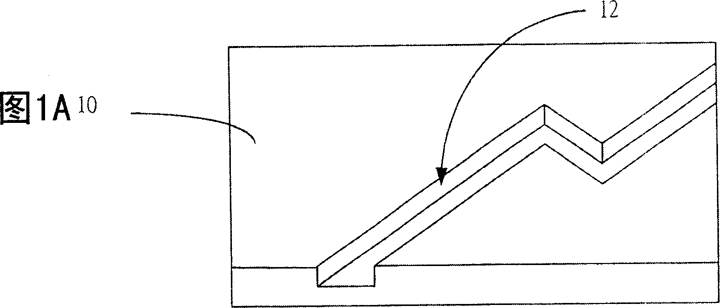
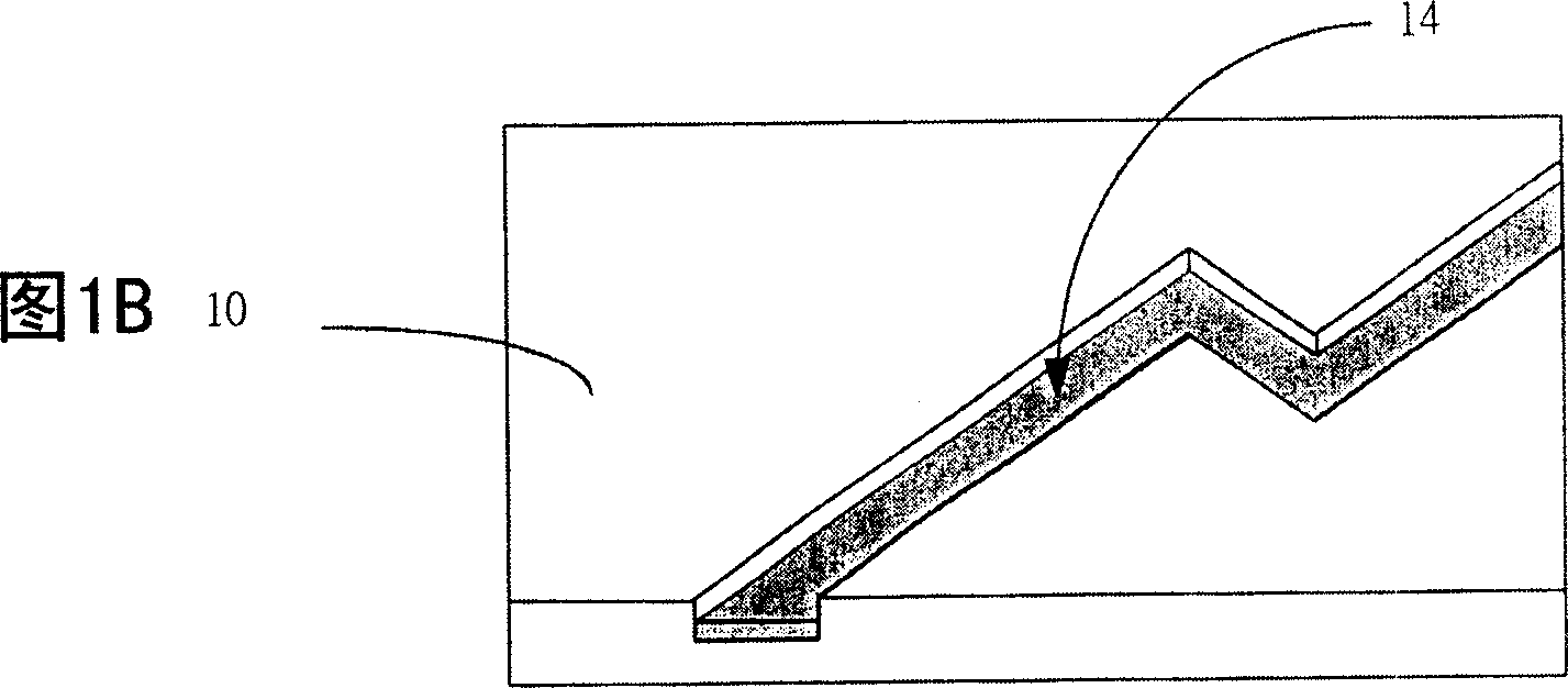
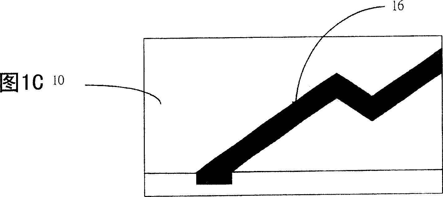
[0015] Please refer to FIGS. 1A-1C . FIGS. 1A-1C are schematic diagrams of a method for manufacturing a conductive circuit according to the present invention. Form the structure of the conductive circuit of the conductive colloid 16 of the present invention as shown in Figure 1C and mainly can be divided into three steps, namely form the groove 12 of the conductive circuit as shown in Figure 1A, form the groove 12 as shown in Figure 1B. The first colloid 14 forms the conductive circuit of the conductive colloid 16 shown in FIG. 1C.

[0016] The conductive colloid 16 is formed by the first colloid 14 and the second colloid (not shown) that will undergo chemical changes with the first colloid 14, and this chemical change makes the second colloid, which is originally in a colloidal state, and the first colloid 14. Form a solid conductive colloid 16 in the groove 12 of the conductive circuit. The first colloid 14 and the second colloid used in the present invention may be Electri...


PUM


Abstract

The method comprises: in the first, providing an insulated baseboard; etching a groove of circuit on the insulated baseboard; filling in a first colloid in the groove of circuit used for generating bridge-erecting action with the insulated colloid; finally, filling in a second colloid capable of generating chemical reaction with the first colloid to form a wire colloid in the groove of circuit.

Description

technical field [0001] The invention relates to a manufacturing method and structure of a conductive circuit, especially a conductive circuit of conductive colloid formed by a first colloid and a second colloid. Background technique [0002] The printed circuit board is a circuit board composed of drawing the electrical wiring connecting the circuit parts into a wiring pattern according to the circuit design, and then reproducing the electrical conductor on the insulator by the mechanical processing and surface treatment specified by the design. In other words, the printed circuit board refers to the substrate before it is equipped with electronic components. [0003] In the known printed circuit board, the conductive circuit is formed by first pasting the copper foil layer on the insulating substrate, and then using procedures such as drilling, developing and etching. [0004] However, in this known method, the insulation value between the lines is not high enough because ...

Claims


Application Information

Patent Timeline
IPC IPC(8): H05K3/10H05K1/02
Inventor 何建汉
Owner 何建汉
Why Eureka
Try Eureka