Semiconductor integrated circuit

An integrated circuit and semiconductor technology, applied in the direction of semiconductor devices, circuits, semiconductor/solid device components, etc., can solve problems such as difficulty in ensuring capacitance, inability to form large capacitors, and inability to provide sufficient electrode area

Inactive Publication Date: 2007-05-16
KAWASAKI MICROELECTRONICS
View PDF3 Cites 5 Cited by
  • Summary
  • Abstract
  • Description
  • Claims
  • Application Information

AI Technical Summary

Problems solved by technology

There is a problem of not being able to provide a sufficient electrode area from a structural point of view and making it difficult to secure a sufficiently large capacitance, especially a problem that a large capacitor cannot be formed when the number of signal wirings increases

Method used


Image

  • Semiconductor integrated circuit
  • Semiconductor integrated circuit
  • Semiconductor integrated circuit

Examples


Embodiment Construction

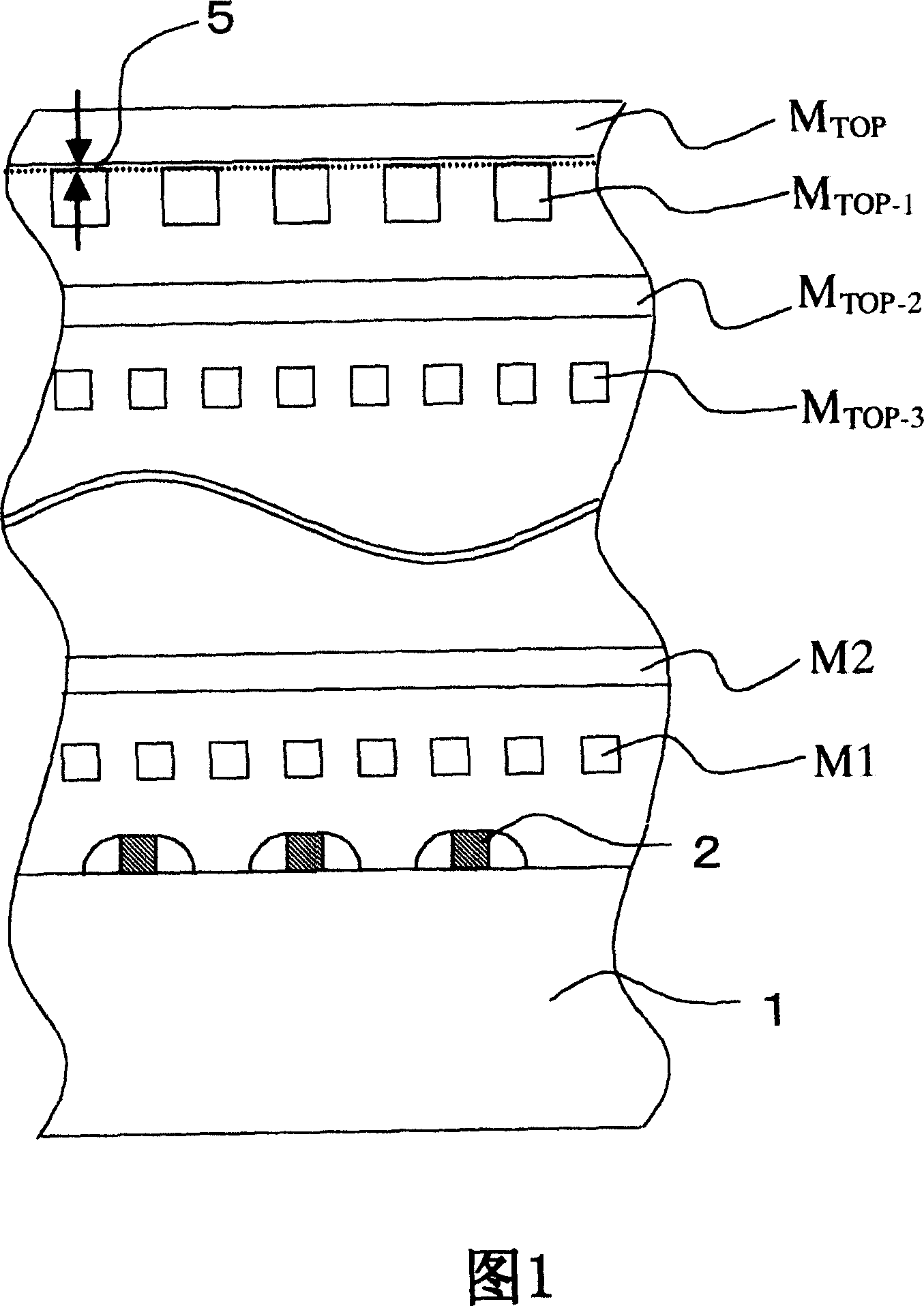
[0020] Various exemplary embodiments are described in detail below. FIG. 1 is a cross-sectional view showing a semiconductor integrated circuit according to an exemplary embodiment. As shown in FIG. 1, the semiconductor integrated circuit includes: a plurality of elements 2, such as MOSFETs, formed on the surface of a semiconductor substrate 1; and metal wiring layers, such as M1 and M2, for connecting the elements together to Make predetermined semiconductor integrated circuits work. These semiconductor integrated circuits are connected by metal wiring included in the metal wiring layer.

[0021] FIG. 1 shows a semiconductor integrated circuit having a multilayer wiring structure including a metal wiring layer M as the above-mentioned metal wiring layer 1 to M TOP . The top metal wiring layer (M TOP ) includes a plurality of top-layer power wirings extending in a first direction. directly on the top metal wiring layer M TOP The next top metal wiring layer below (M TOP...


PUM


Abstract

A semiconductor integrated circuit having a multilayer wiring structure is provided which includes: a top metal wiring layer (MTOP) including a plurality of top layer power supply wirings and a next-to-top metal wiring layer (MTOP-1) directly below the top metal wiring layer MTOP including a plurality of next-to-top layer power supply wirings. Each of the top layer and the next-to-top layer power supply wirings also includes first potential wirings for supplying a first potential to the circuit elements and second potential wirings for supplying a second potential to the circuit elements. The top layer power supply wirings and the next-to-top layer power supply wirings cross each other and have a top layer insulating film disposed between them. First and second contacts are provided in the insulating film for connecting the first potential wirings and second potential wirings in the top and the next-to-top metal wiring layers with each other.

Description

[0001] This application claims priority from Japanese Application No. 2005-325508 filed on November 10, 2005, the entire contents of which are hereby incorporated by reference. technical field [0002] The invention relates to a semiconductor integrated circuit operating at low voltage and high speed, in particular to a semiconductor integrated circuit capable of stabilizing the working power supply. Background technique [0003] In a semiconductor integrated circuit, power supply wiring and ground wiring whose resistance is sufficiently reduced are arranged in a circuit for supplying a specific voltage to each element and stably operating each element in the circuit. However, when high power consumption occurs locally in a semiconductor integrated circuit, the power supply voltage drops instantaneously in its vicinity. As a result, operation errors in logic circuits or jitter in output signals occur. This phenomenon remarkably occurs in semiconductor integrated circuits op...

Claims


Application Information

Patent Timeline
Patent Type & Authority Applications(China)
IPC IPC(8): H01L27/04H01L23/522
CPCH01L23/5286H01L23/5223H01L2924/0002H01L2924/00
Inventor 木村吉孝
Owner KAWASAKI MICROELECTRONICS
Why Eureka
Try Eureka