Transfer equipment

A transfer device, plate-shaped body technology, applied in the directions of transportation and packaging, furnace, charge control, etc., can solve the problems of assembly device difficulty, cracking, wafer scratches, etc., avoid damage such as cracking, and shorten the processing time of temperature adjustment. Effect

Inactive Publication Date: 2007-06-13
LINTEC CORP
View PDF1 Cites 13 Cited by
  • Summary
  • Abstract
  • Description
  • Claims
  • Application Information

AI Technical Summary

Problems solved by technology

[0005] However, in the structure disclosed in Patent Document 1, only the front end side of the arm is moved to push the suction portion onto the wafer for suction and holding when transferring the wafer, which causes the following problems
[0006] That is, recent wafers, for example, are ground to a thickness of tens of μm order, so when the parallelism between the support surface of the support plate and the wafer surface deviates, that is, when a slight inclination occurs, there is a gap between the support plate and the wafer surface. When the surfaces of the wafers are in contact, a local load may be applied to the wafer, which may cause damage such as scratches or cracks on the wafer, causing such abnormal problems
In addition, it is very difficult to assemble the device while maintaining the parallelism of the support plate with respect to the wafer with high precision. At the same time, the accuracy of the components used is also strictly required, which also brings a heavy burden in terms of cost.

Method used


Image

  • Transfer equipment
  • Transfer equipment
  • Transfer equipment

Examples


Embodiment Construction

[0038] Hereinafter, embodiments of the present invention will be described with reference to the drawings.

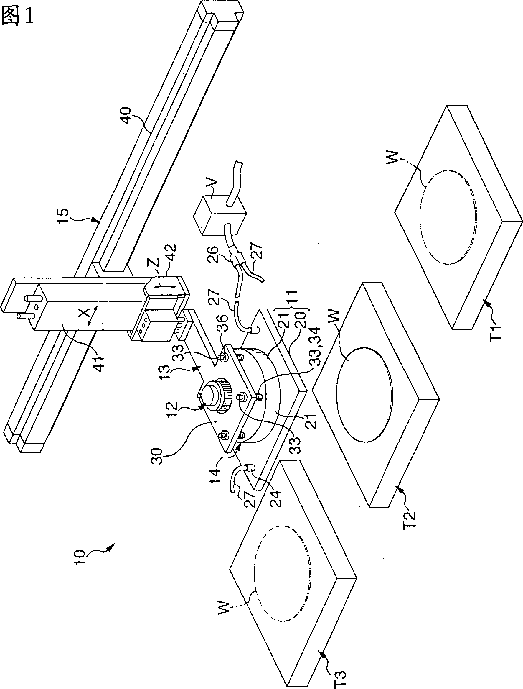
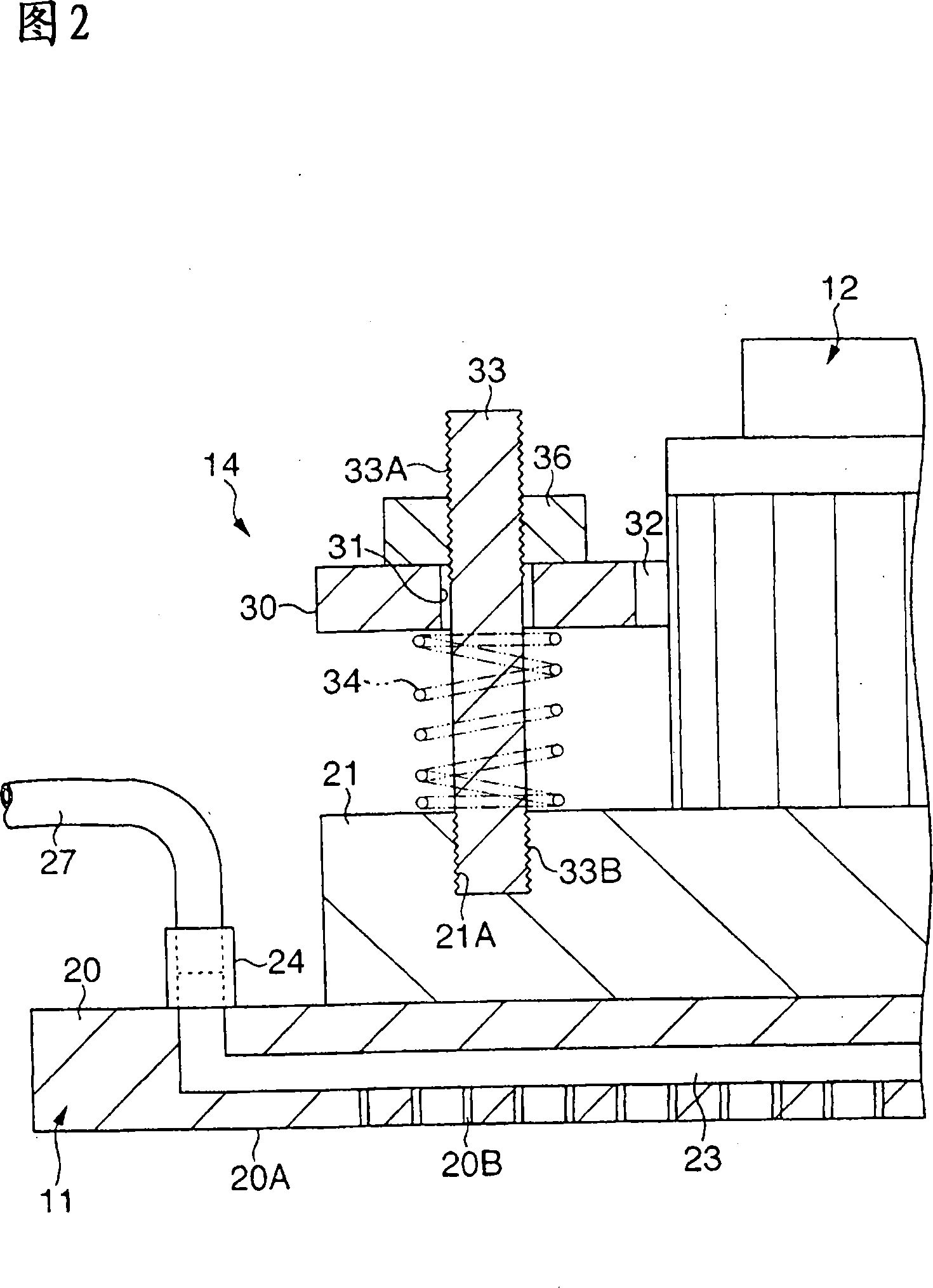
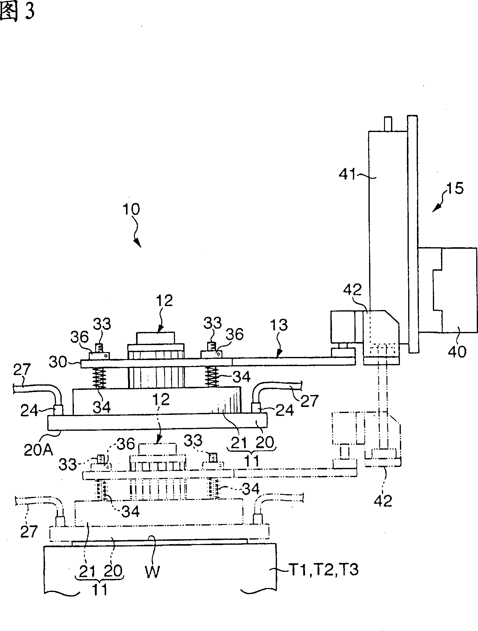
[0039] The schematic structure of the transfer apparatus of this embodiment is shown in FIG. 1. As shown in FIG. In this figure, the transfer device 10 includes a support plate 11 for a wafer W as a plate-shaped body, a temperature adjustment device 12 for adjusting the temperature of the support plate 11, and a holding member 13 for holding the support plate 11. A parallelism adjustment mechanism 14 between the support plate 11 and the holding member 13, and a moving device 15 for moving the support plate 11 in the X and Z directions in FIG. 1 .

[0040] First to third stages T1 , T2 , and T3 are disposed below the support plate 11 , and a wafer W is transferred between these stages T1 to T3 by a transfer device 10 . These stages T1 to T3, whose detailed structures are omitted here, include means for controlling the temperature of the wafer W to a predetermined temper...


PUM


Abstract

Transfer equipment (10) is provided with a supporting plate (11) which has a supporting plane (20A) for a semiconductor wafer (W), an arm plate (30) for supporting the supporting plate, and a parallelism adjusting means (14) arranged between the supporting plate and the arm plate (13). The supporting plate is arranged to permit air to be sucked and discharged from the supporting plane, is maintained parallel to the wafer by the reaction when the supporting plate is brought close to the semiconductor wafer (W) in a status where air is discharged. After the supporting plate is brought into contact with the wafer in a status where the parallelism is maintained, the supporting plate sucks the wafer and transfers it.

Description

technical field [0001] The present invention relates to a transfer device, and particularly relates to a transfer device suitable for suction transfer without damaging a brittle plate-shaped object such as a semiconductor wafer ground to an extremely thin state. Background technique [0002] As a semiconductor wafer (hereinafter simply referred to as "wafer") on which a circuit surface is formed, it is necessary to perform heat-sensitive adhesive bonding for die bonding on the back side with a protective tape attached to the circuit surface. A series of processing such as splices, and then installed on the ring frame. Such a device for performing a series of processes is disclosed in Patent Document 1, for example. [0003] In Patent Document 1, an arm-type transfer device is used as a device for transferring a wafer to each process. In this transfer device, a suction unit is provided on the front end side of the arm, and the wafer can be supported and transferred to a pre...

Claims


Application Information

Patent Timeline
Patent Type & Authority Applications(China)
IPC IPC(8): H01L21/68B25J15/06B65G49/07
CPCB25J9/023B25J15/0616H01L21/6838B25J17/0208H01L21/68
Inventor 坂本和纪小林贤治
Owner LINTEC CORP
Why Eureka
Try Eureka