Electronic device with grounding structure

An electronic device and grounding structure technology, applied in the direction of digital processing power distribution, etc., can solve the problems of complex grounding structure, and achieve the effect of simplifying the structure, reducing the cost, and reducing the contact area.

Inactive Publication Date: 2007-06-20
INNOCOM TECH SHENZHEN +1
View PDF0 Cites 5 Cited by
  • Summary
  • Abstract
  • Description
  • Claims
  • Application Information

AI Technical Summary

Problems solved by technology

[0009] In order to overcome the defects of the complex grounding structure of the circuit board in the prior art, it is necessary to provide an electronic device with a simple structure and a grounding structure

Method used


Image

  • Electronic device with grounding structure
  • Electronic device with grounding structure
  • Electronic device with grounding structure

Examples


Embodiment Construction

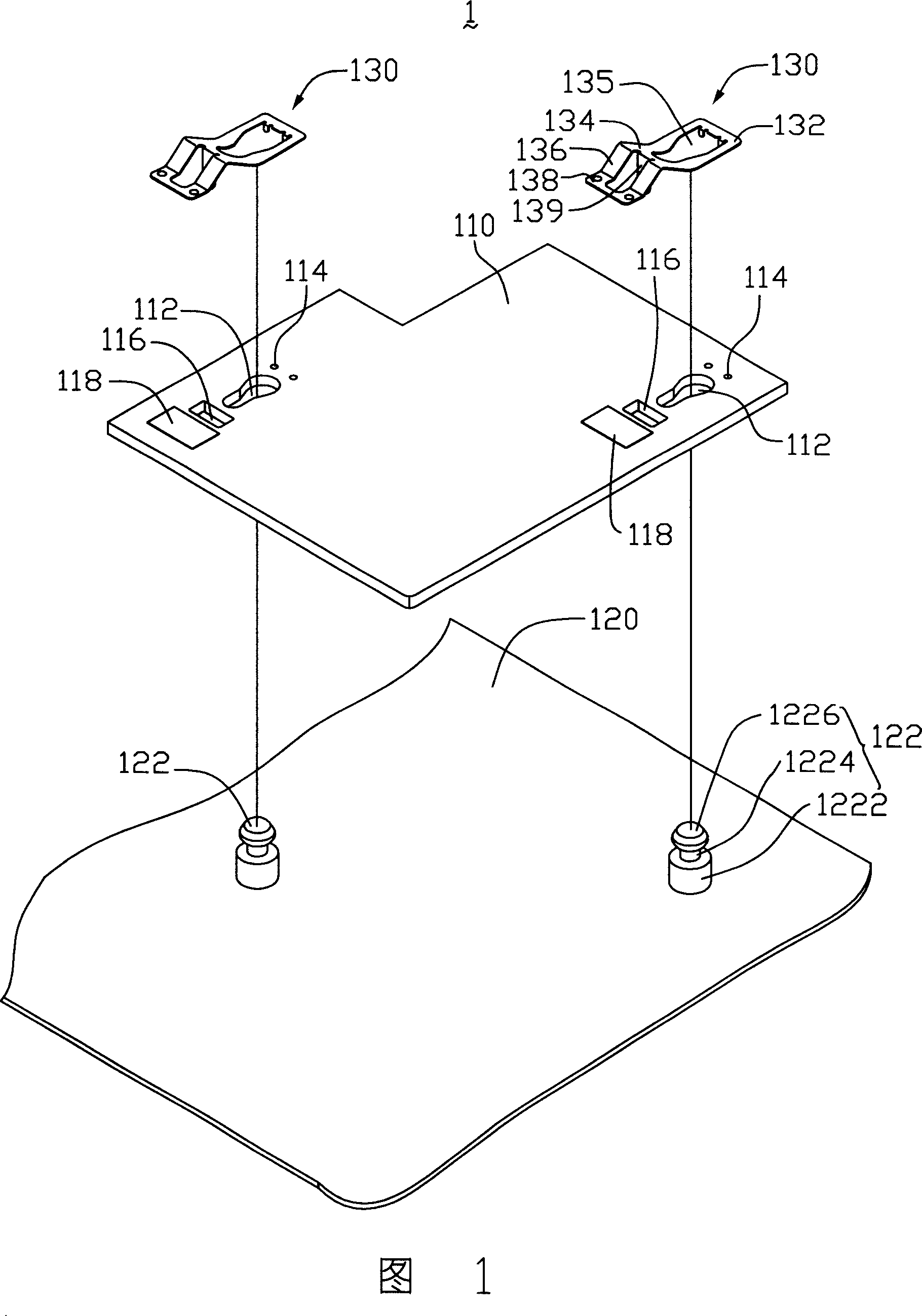
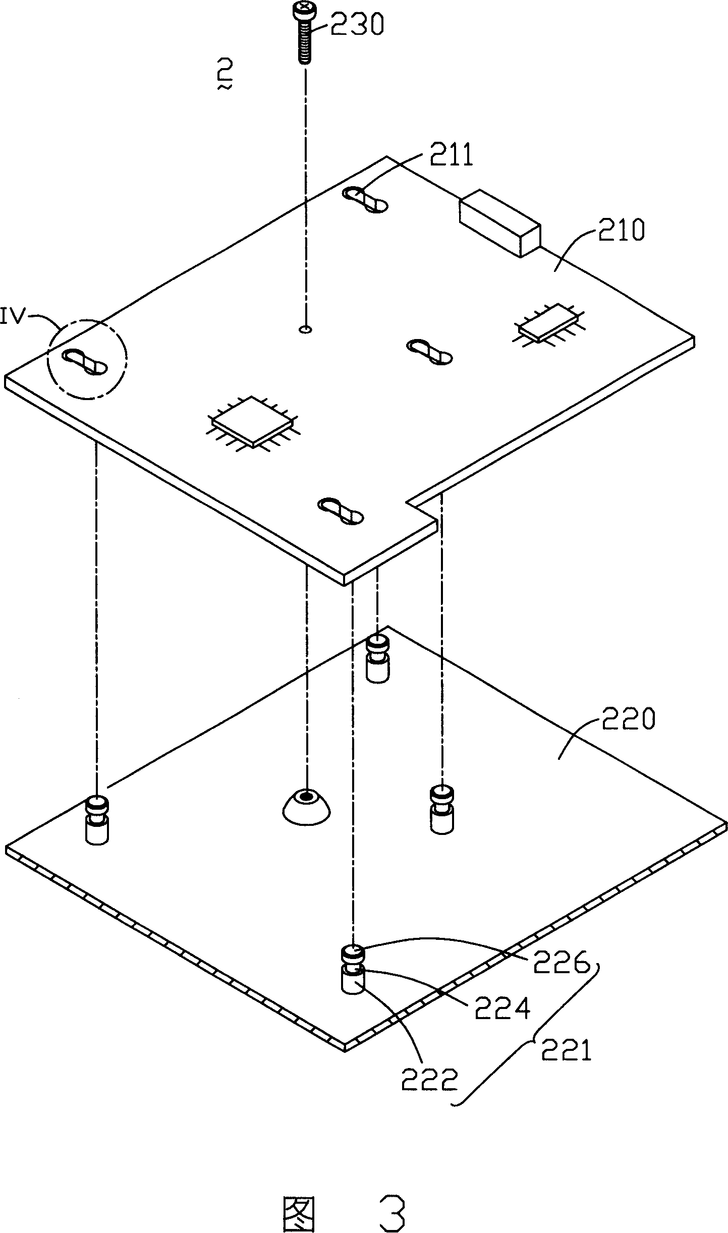
[0018] Please refer to FIG. 3 and FIG. 4 , FIG. 3 is a schematic diagram of a first embodiment of an electronic device with a grounding structure according to the present invention, and FIG. 4 is an enlarged view of part IV shown in FIG. 3 . The electronic device 2 with a grounding structure includes a carrier board 220 and a circuit board 210 fixed on the carrier board 220 , and the carrier board 220 is conductive.

[0019] The circuit board 210 includes at least one through hole 211, the through hole 211 includes an introduction hole 214 and a buckle hole 212, the diameter of the introduction hole 214 is larger than the diameter of the buckle hole 212, a ground layer is arranged around the buckle hole 212 215, the ground layer 215 is solder.

[0020] The carrier plate 220 is provided with at least one fixing column 221 corresponding to the perforation 211, and the fixing column 221 can conduct electricity, which includes a column part 222, a head 226, and the head 226 and th...


PUM


Abstract

An electronic device with grounding structure consists of a conductive load-carry board with a conductive fixing column and a circuit board with a through hole. It is featured as arranging a grounding layer at periphery of said through hole, checking said fixing column into said through hole for fixing said circuit board and connecting said fixing column with said grounding layer.

Description

【Technical field】 [0001] The invention relates to an electronic device with a grounding structure. 【Background technique】 [0002] The circuit board in a general computer or server is the core part of the computer system, and its fixing in the electronic device will affect the performance of the computer system. When fixing the circuit board, it is necessary to prevent the solder joints of the electronic components on the circuit board from contacting the computer case to cause a short circuit on the circuit board, and at the same time, the circuit board needs to be grounded. [0003] In order to solve the above problems, an electronic device 1 used in the prior art can refer to FIG. fixed on the carrier board 120. [0004] A plurality of through holes 112 are disposed on the circuit board 110 , two positioning holes 114 are disposed on one side of the through holes 112 , and a through hole 116 is disposed on the other side. A ground plate 118 is disposed on the circuit b...

Claims


Application Information

Patent Timeline
Patent Type & Authority Applications(China)
IPC IPC(8): G06F1/18
Inventor 林国庆陈威钧张祥
Owner INNOCOM TECH SHENZHEN
Why Eureka
Try Eureka