Transistor epitaxial wafer and transistor
A technology for epitaxial wafers and transistors, which is applied to transistors, semiconductor devices, electrical components, etc., can solve the problems of poor surface flatness and high diffusion coefficient of the non-alloy layer 14, and achieve low power consumption, good resistance, and reduced resistance. Effect
- Summary
- Abstract
- Description
- Claims
- Application Information
AI Technical Summary
Problems solved by technology
Method used
Image

Examples
no. 1 Embodiment approach
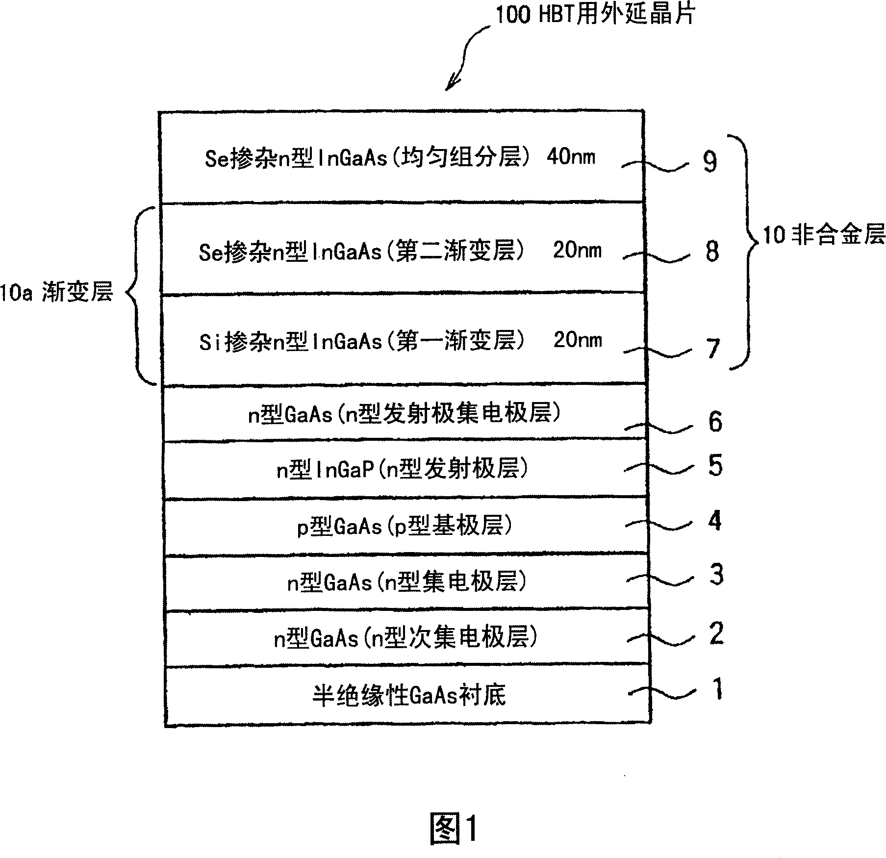
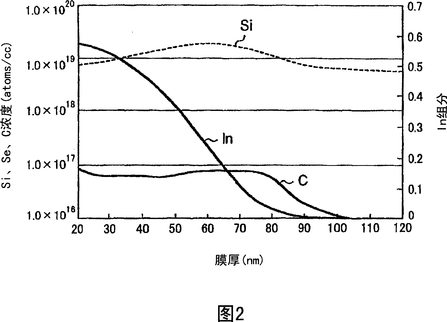
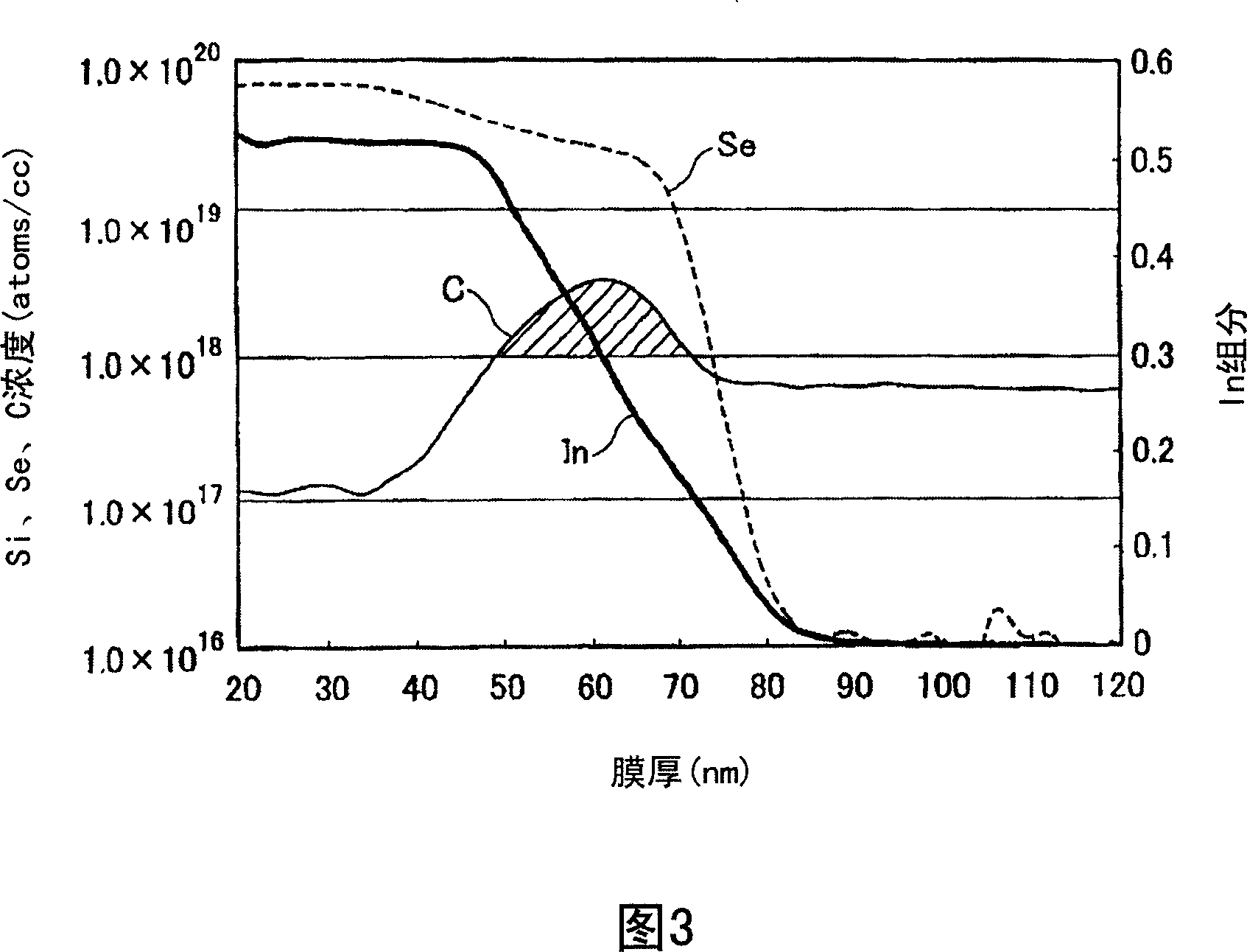
[0101] FIG. 1 shows an epitaxial wafer for HBT according to a first embodiment of the present invention. The HBT epitaxial wafer 100 is obtained on the basis of the above results, and the In in the n-type InGaAs non-alloy layer 10 0→x Ga 1→1-x In the graded As layer 10a, Si is used as the dopant between In composition 0-0.35, and Se is doped for the remaining In composition between 0.35 and uniform In composition.
[0102] The structure of the epitaxial wafer 100 for HBT is that on the semi-insulating GaAs substrate 1, n-type GaAs layers (for example, thickness 500nm, carrier concentration 3×10 18 cm -3 ) composed of n-type sub-collector layer 2, composed of n-type GaAs layer (for example, thickness 700nm, carrier concentration 1×10 16 cm -3 ) composed of n-type collector layer 3, composed of p-type GaAs layer (for example, thickness 80nm, carrier concentration 4×10 19 cm -3 ) The p-type base layer 4 composed of n-type In x Ga 1-x P layer (X=0.48) (for example, thickne...
no. 2 Embodiment approach
[0115] FIG. 5 shows an HBT according to a second embodiment of the present invention. This HBT 200 is formed using the epitaxial wafer of the first embodiment shown in FIG. 1 .
[0116] The main body of HBT200 is composed of an epitaxial wafer. The structure of this epitaxial wafer is that on a semi-insulating GaAs substrate 1, an n-type sub-collector layer 2 composed of an n-type GaAs layer is sequentially stacked, and an n-type sub-collector layer 2 composed of an n-type GaAs layer is sequentially stacked. type collector layer 3, p-type base layer 4 composed of p-type GaAs layer, composed of n-type In x Ga 1-x An n-type emitter layer 5 composed of a P layer (X=0.48), an n-type emitter-collector layer 6 composed of an n-type GaAs layer, and an n-type InGaAs non-alloy layer 10 .
[0117] The n-type InGaAs non-alloy layer 10 consists of a first graded layer 7 doped with Si, a second graded layer 8 doped with Se, and an n-type In layer doped with Se. x Ga 1-x The homogeneous...
Embodiment approach
[0122] In addition, this invention is not limited to each said embodiment, Various deformation|transformation is possible in the range which does not deviate from or change the technical idea of this invention.
[0123] For example, in the above-mentioned embodiment, the In composition of the uniform composition layer 9 is fixed at 0.5, but the In composition may be fixed at any value from 0.4 to 0.7.
[0124] In addition, the case where the n-type InGaAs heterogeneous composition layer (graded layer 10a) is a linearly graded layer in which the In composition gradually increases from 0 has been described, but it may also be a stepwise change in the In composition. gradient layer. Furthermore, instead of a gradient layer, the In composition of the first layer is in the range of 0 to 0.35, and the In composition of the second layer is inhomogeneous in the range of 0.35 to the In composition value of the uniform composition layer. layer.
[0125] in addition. In the above em...
PUM
 Abstract
Description
Claims
Application Information
 - R&D Engineer
- R&D Manager
- IP Professional
- Industry Leading Data Capabilities
- Powerful AI technology
- Patent DNA Extraction
Browse by: Latest US Patents, China's latest patents, Technical Efficacy Thesaurus, Application Domain, Technology Topic.
© 2024 PatSnap. All rights reserved.Legal|Privacy policy|Modern Slavery Act Transparency Statement|Sitemap