Film etching method

A thin film and etchant technology, applied in the field of thin film etching, can solve the problems of increased contact area, chamfering or imperfect film shape, etc., to achieve the effect of improving the coating ability

Inactive Publication Date: 2007-07-04
CHUNGHWA PICTURE TUBES LTD
View PDF0 Cites 8 Cited by
  • Summary
  • Abstract
  • Description
  • Claims
  • Application Information

AI Technical Summary

Problems solved by technology

[0007] The purpose of the present invention is to adjust the steps of thin film manufacturing. By adding an etching process of stripping the photoresist, the contact area between the thin film and the etching material is increased, so that the chamfer produced by the existing etching process can be eliminated. or problems with imperfect film shape

Method used


Image

  • Film etching method
  • Film etching method
  • Film etching method

Examples


Embodiment Construction

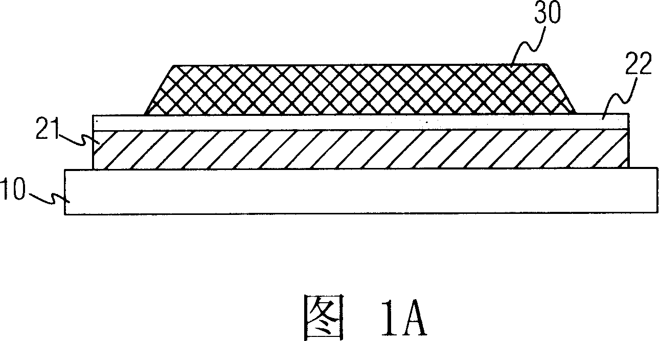
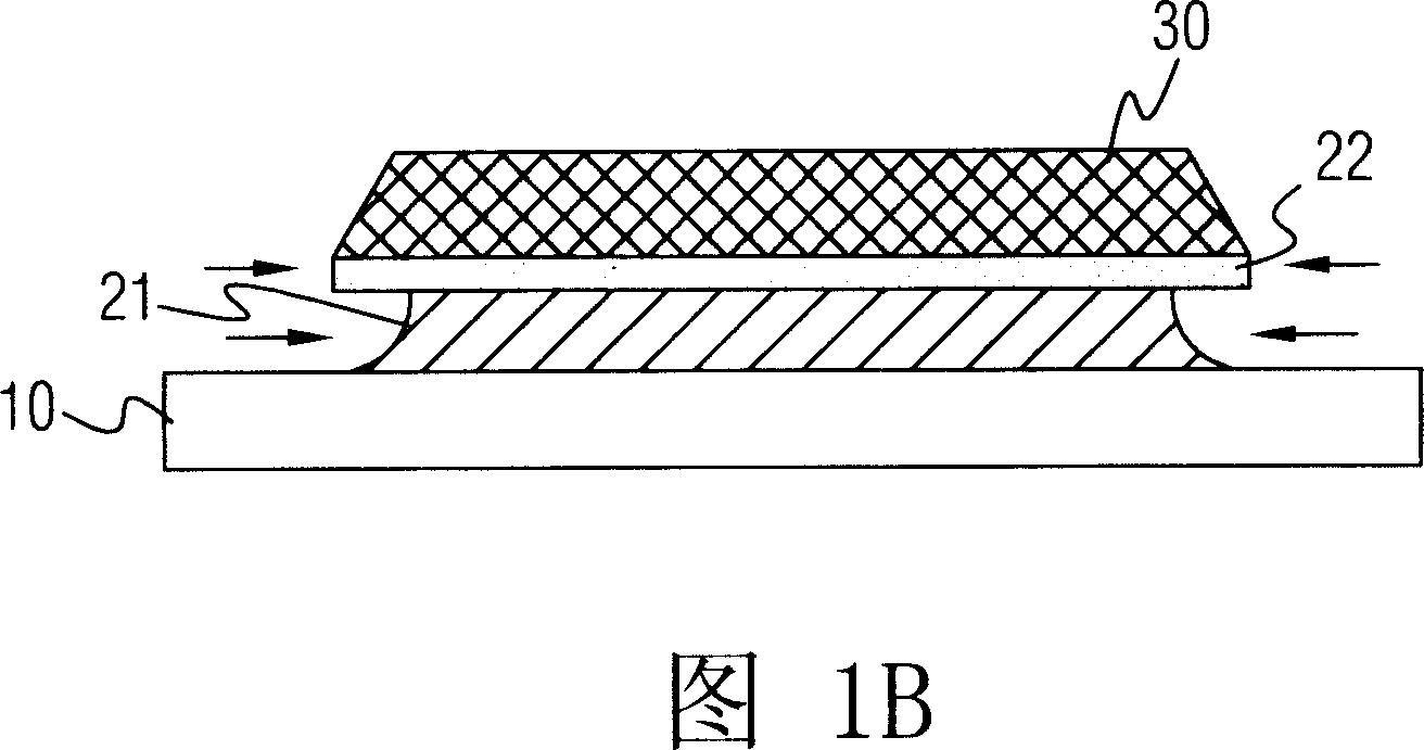
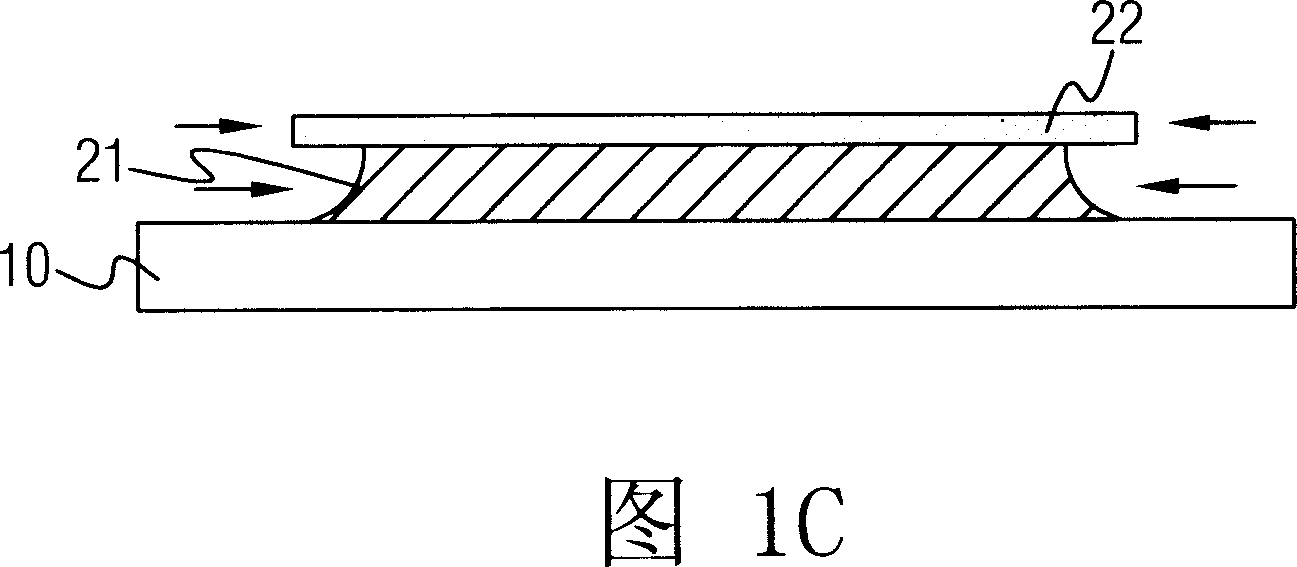
[0054] As shown in FIG. 4 , it is a flowchart of an embodiment of a thin film etching method of the present invention. The thin film etching method is applied in the thin film manufacturing process of a semiconductor or a thin film transistor array, and comprises the following steps: providing a substrate on which at least one thin film is formed, and on the top of the uppermost layer of the thin film A photoresist is formed (step S1); the first stage etching is to use the first etchant to etch the film (step S2); the second stage etching is to use The second etchant etches the photoresist (step S3); and the third stage etching is to etch the film again with the first etchant after the second stage etching (step S4 ).

[0055] As shown in FIG. 5A , it is a schematic structural view of a double-layer film structure after photolithography. As shown in FIG. 5B , it is a schematic diagram of the first-stage etching for the double-layer film structure in FIG. 5A . As shown in FI...


PUM


Abstract

This invention is a thin film etching method, being applied to a semiconductor or thin film transistor array (TFT Array) film process, to improve the undercut problem of existing etching, or make the etched film's shape more perfect. The film etching method divides the existing etching process into two stages, and between the two stages, inserting into a photoresist etching process, and through appropriate photoresist etching, it increases the contact area of the film and the etching materials, so that it can eliminate the existing etching problem that the undercut or file shape is not perfect.

Description

technical field [0001] The present invention relates to a thin film etching method, in particular to a thin film etching method applied in the thin film manufacturing process of semiconductor or thin film transistor arrays to eliminate chamfering after etching or improve the imperfect shape of the thin film after etching method. Background technique [0002] When using thin-film technology to manufacture electronic components or wires, there are generally multiple processes such as film formation, photoresist, and etching according to the characteristics of the manufactured components, and the etching is to use chemical reactions or physical impacts on materials. The technology of removal by action can achieve specific functions by forming the film into a specific structural shape by etching. Etching techniques can be divided into two types: Wet Etching and Dry Etching. In wet etching, chemical solution is used to achieve the purpose of etching through chemical reaction, w...

Claims


Application Information

Patent Timeline
Patent Type & Authority Applications(China)
IPC IPC(8): H01L21/00H01L21/3213C23F1/02C23F1/16
Inventor 许嘉哲施雅钟郑勉仁吴承昌张瑞宗
Owner CHUNGHWA PICTURE TUBES LTD
Why Eureka
Try Eureka