
Method for manufacturing cmos image sensor

An image sensor and pattern technology, applied in semiconductor/solid-state device manufacturing, electrical solid-state devices, semiconductor devices, etc., can solve problems such as threshold voltage fluctuations

Inactive Publication Date: 2007-07-04
DONGBU ELECTRONICS CO LTD
View PDF0 Cites 3 Cited by
  • Summary
  • Abstract
  • Description
  • Claims
  • Application Information

AI Technical Summary

Problems solved by technology

Due to the plasma effect, the fluctuation of the threshold voltage Vth becomes quite severe, thereby causing considerable problems in controlling the stability of the device

Method used


Image

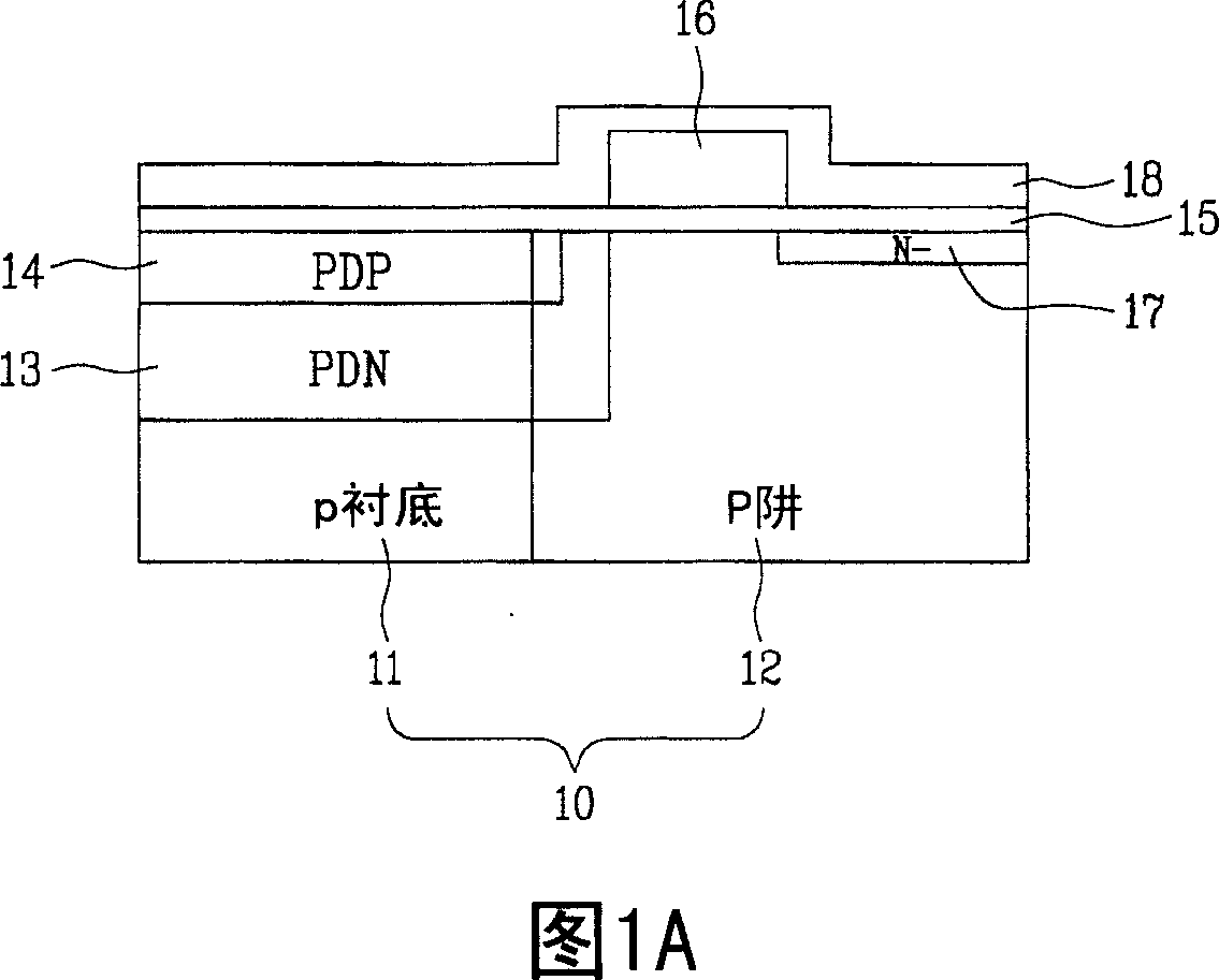
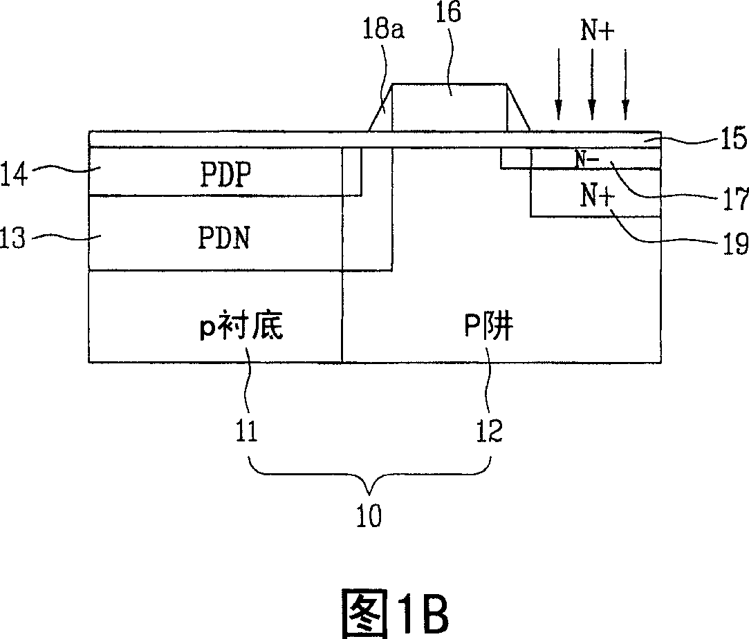
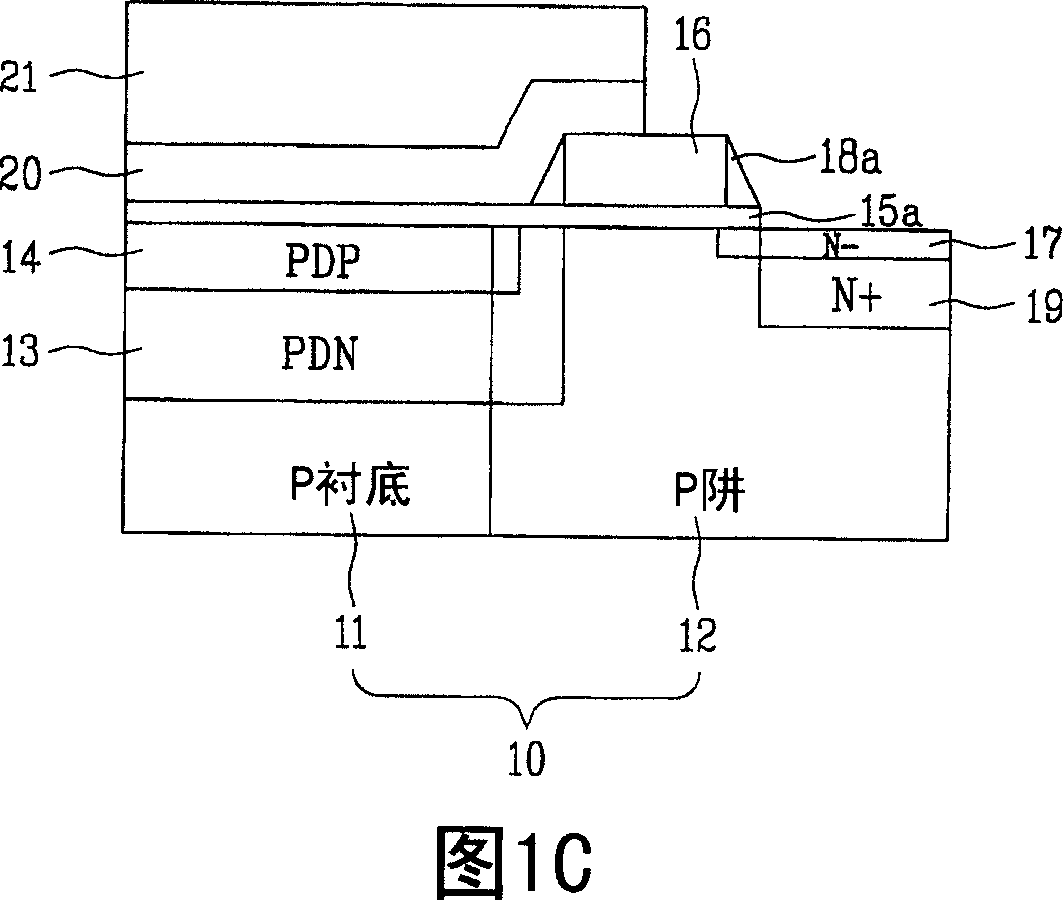
  • Method for manufacturing cmos image sensor
  • Method for manufacturing cmos image sensor
  • Method for manufacturing cmos image sensor

Examples


Embodiment Construction

[0034] Preferred embodiments of the invention will be described in detail hereinafter, examples of which are illustrated in the accompanying drawings.

[0035] 2A to 2D are cross-sectional views illustrating a manufacturing method of manufacturing a CIS according to the present invention.

[0036] Referring to FIG. 2A, an STI (not shown) is formed on a semiconductor substrate 100 formed of an epitaxial layer. By forming the STI, the device isolation region is separated from the active region.

[0037] Subsequently, P-type impurities are implanted into the active region portion to form the P well 102 , wherein the active region portion belongs to the portion of the semiconductor substrate 100 other than the STI region. The active region portion is defined in a portion of the semiconductor substrate 100 other than the portion where the PD is to be formed. Here, other regions where the P well 102 is not formed are defined as the P subsubstrate 101 .

[0038] Subsequently, an o...


PUM


Abstract

The invention provides a method for manufacturing a CIS, wherein a process has been improved in order to reduce or prevent a dark current of a photodiode region. In the method, a plurality of gates are formed on a semiconductor substrate, and impurities are implanted in side portions of a predetermined gate to form a photodiode region. Subsequently, a spacer nitride layer is formed and then etched to form a first spacer pattern covering the photodiode region and a second spacer pattern on sidewalls of the rest of the gates. After that, impurities are implanted using the first and second spacer patterns as a mask to form source / drain regions in portions of the semiconductor substrate that are exposed at the side portions of the gate(s). Subsequently, a salicide is formed on the gate and in the exposed portion of the semiconductor substrate.

Description

technical field [0001] The present invention relates to a complementary metal-oxide-semiconductor image sensor (CMOS), and more particularly to a method of manufacturing a CMOS image sensor, wherein the process is improved in order to prevent dark current in a photodiode region. Background technique [0002] In general, an image sensor is a semiconductor device that converts an optical image into an electrical signal. Image sensors are roughly classified into Charge Coupled Devices (CCD) and CMOS Image Sensors (CSI). [0003] CCD not only has a complicated driving method, but also consumes a lot of power, and requires multiple masking processes. In addition, the CCD also has the disadvantage that the signal processing circuit cannot be implemented inside the CCD chip, so it is difficult to manufacture the CCD on a single chip. Therefore, CIS using CMOS manufacturing technology has recently attracted attention. [0004] Hereinafter, a method of manufacturing a CIS accordin...

Claims


Application Information

Patent Timeline
Patent Type & Authority Applications(China)
IPC IPC(8): H01L21/822H01L27/146
CPCH01L27/14603H01L27/14689
Inventor 奇安度
Owner DONGBU ELECTRONICS CO LTD
Learn More