
Programmable logic device, method for verifying error of programmable logic device, and method for forming circuit of programmable logic device

a programmable logic and error detection technology, applied in logic circuits using specific components, pulse techniques, instruments, etc., can solve problems such as error in the arithmetic operation result of the arithmetic operation circuit, and achieve the effect of improving the error detection ra

Active Publication Date: 2018-09-04
CONTROL SYST LAB LTD
View PDF9 Cites 0 Cited by
  • Summary
  • Abstract
  • Description
  • Claims
  • Application Information

AI Technical Summary

Benefits of technology

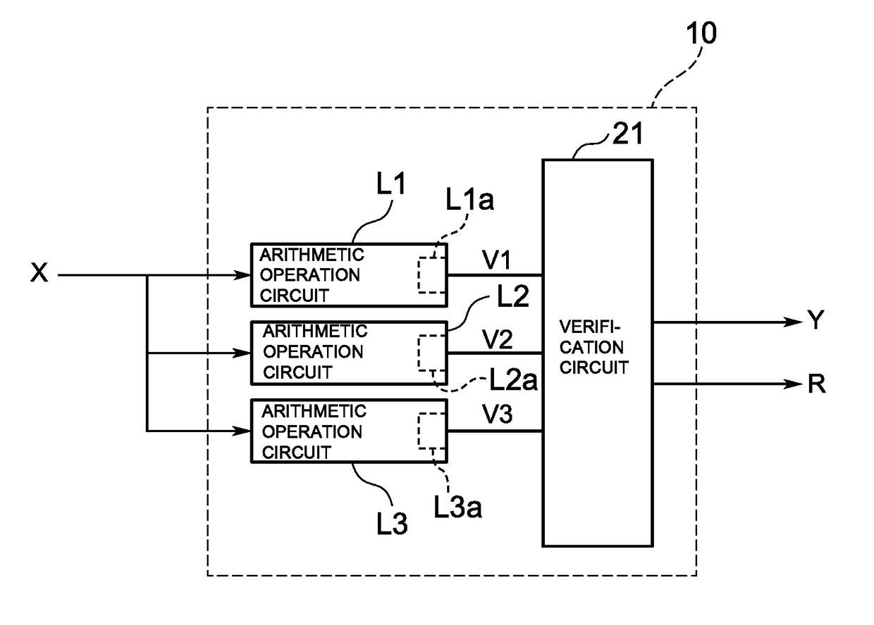
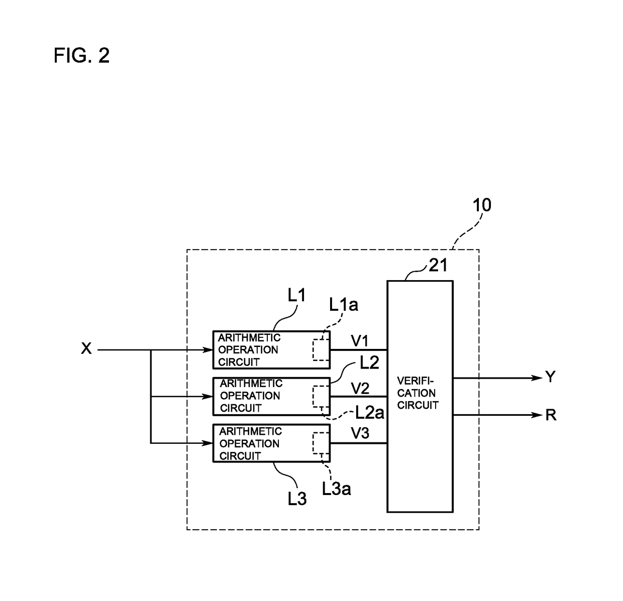
The present invention relates to a programmable logic device and a method for verifying an error of the device. The device has multiple arithmetic operation circuits that vary in their operating state and error occurrence state due to common factors such as temperature, voltage, and clock fluctuations. By comparing the results of these circuits, the device can detect errors caused by these factors and improve error detection compared to conventional devices. The invention also allows for the formation of circuits with different combinations of circuit blocks, further increasing the error detection rate.

Problems solved by technology

The circuit elements such as an AND gate, and an OR gate may cause malfunctions due to charged particles or the like in the atmosphere.
In a case where the circuit elements incorporated into the arithmetic operation circuit malfunction, for example, the arithmetic operation result of the arithmetic operation circuit is in error.

Method used


Image

  • Programmable logic device, method for verifying error of programmable logic device, and method for forming circuit of programmable logic device
  • Programmable logic device, method for verifying error of programmable logic device, and method for forming circuit of programmable logic device
  • Programmable logic device, method for verifying error of programmable logic device, and method for forming circuit of programmable logic device

Examples


Embodiment Construction

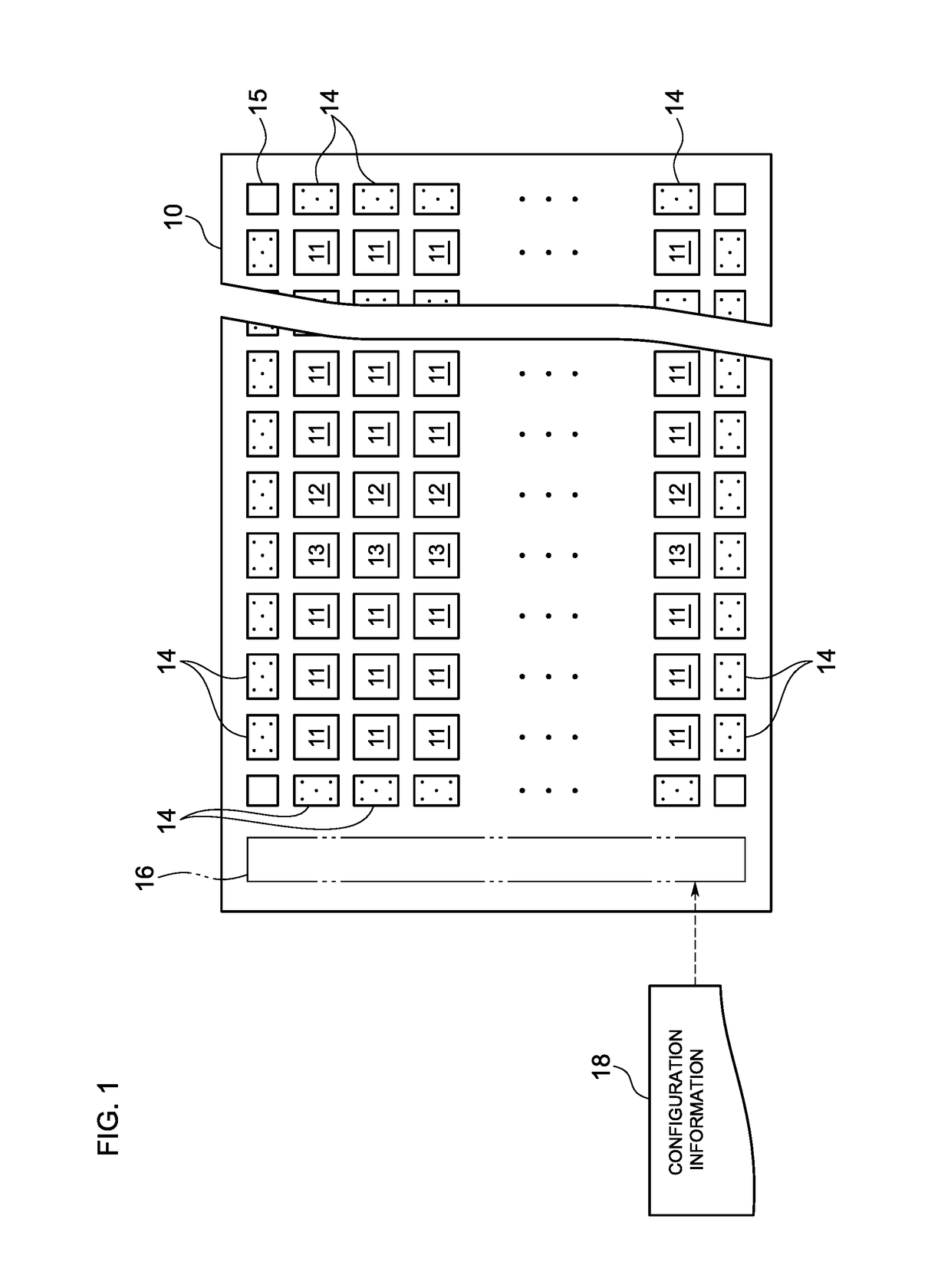
[0022]FIG. 1 illustrates an FPGA (Field Programmable Gate Array) 10 used in the present embodiment. The present embodiment describes a case where the present invention is applied to the general FPGA 10 as an example of a programmable logic device (PLD). The FPGA 10 is a device capable of changing arithmetic operation functions such as a communication processing function, an encryption processing function, and an image processing function. The FPGA 10 includes circuit blocks (circuit elements) such as basic logic blocks 11, DSP blocks 12, block RAMS 13, IO blocks (Input / Output Blocks) 14, and PLL blocks 15 to provide the desired arithmetic operation functions in accordance with types of signals to be subjected to arithmetic processing and contents of the arithmetic processing. The FPGA 10 includes a configuration memory 16, and routing resources (not illustrated) for connecting between circuit blocks, in addition to the circuit blocks.

[0023]The basic logic block 11 is a basic circuit...


PUM


Abstract

Arithmetic operation circuits and a verification circuit are formed by loading configuration information into a configuration memory in an FPGA. Arithmetic operation circuits have the same arithmetic operation function, but are different from each other in combination of the circuit blocks. The arithmetic operation circuits are formed by combining the circuit blocks to make the maximum use of the DSP block, while the arithmetic operation circuit is formed by combining the circuit blocks other than DSP block. The arithmetic operation circuits each are configured to use a block RAM as the data hold memory, while the arithmetic operation circuit is configured to use a distributed RAM as the data hold memory. Each of the arithmetic operation circuits receives the input data, and outputs arithmetic operation result data (V1 to V3). A verification circuit compares the arithmetic operation result data to verify whether errors occur.

Description

CROSS REFERENCE TO RELATED APPLICATION[0001]The present application claims benefit of International Patent Application (PCT) No. PCT / JP2016 / 055389 filed on Feb. 24, 2016, which claims priority to Japanese Patent Application No. 2015-094970 filed on May 7, 2015. Both of the aforementioned applications are incorporated herein by reference in their entireties.TECHNICAL FIELD[0002]The present invention relates to a programmable logic device, a method for verifying an error of the programmable logic device, and a method for forming a circuit of the programmable logic device.BACKGROUND ART[0003]In recent years, programmable logic devices, especially FPGAs (Field Programmable Gate Arrays) have been frequently used in control and communication fields. The FPGA includes an arithmetic operation circuit formed by combining circuit blocks such as basic logic blocks (also referred to as CLBs (Configurable Logic Blocks), LEs (Logic Elements) or the like) in accordance with configuration informati...

Claims


Application Information

Patent Timeline
Patent Type & Authority Patents(United States)
IPC IPC(8): G06F13/00G06F7/02H03K19/173G06F7/483
CPCG06F7/02H03K19/173G06F7/483H03K19/17724
Inventor MORIMOTO, KENICHI
Owner CONTROL SYST LAB LTD
Learn More