Clock duty cycle calibration and frequency multiplier circuit

a frequency multiplier and clock duty cycle technology, applied in logic circuits characterised by logic functions, pulse techniques, frequency change manipulation, etc., can solve the problems of deteriorating the purity of the output clock signal of a phase-lock loop, implementing clock signal frequency multiplication, and relatively high power consumption, so as to simplify circuit design, small adjustment of step precision, and large dynamic range

Active Publication Date: 2019-01-15
ALLWINNER TECH CO LTD
View PDF11 Cites 5 Cited by
  • Summary
  • Abstract
  • Description
  • Claims
  • Application Information

AI Technical Summary

Benefits of technology

[0005]An objective of the present invention is to provide a clock duty cycle calibration and frequency multiplier circuit, so as to implement high-precision clock signal frequency multiplication with relatively low circuit complexity and low cost.
[0030]Compared with the prior art, a clock duty cycle calibration and frequency multiplier circuit of the present invention implements separation of a frequency multiplication delay unit and a calibration delay unit and simplifies circuit design. The calibration delay unit demands a large dynamic range and a small adjustment of step precision and have no requirement for phase noise performance; and the frequency multiplication delay unit may be fixed delay, and requires only low phase noise design. In this way, optimal design of different circuit modules can be implemented, and power consumption and area consumption are reduced.

Problems solved by technology

This deteriorates purity of the output clock signal of a phase-lock loop.
It can be learned from above that a difficulty of implementing clock signal frequency multiplication lies in calibration of a clock signal duty cycle.
Using an analog circuit to implement calibration of a clock signal duty cycle is of relatively high power consumption and using a digital circuit to implement calibration of a clock signal duty cycle faces compromised restriction of a plurality of aspects such as phase noise, area, and dynamic range.

Method used


Image

  • Clock duty cycle calibration and frequency multiplier circuit
  • Clock duty cycle calibration and frequency multiplier circuit
  • Clock duty cycle calibration and frequency multiplier circuit

Examples


Embodiment Construction

[0037]A clock duty cycle calibration and frequency multiplier circuit according to the present invention is used to perform delay, comparison, and a logic operation on a clock signal, so as to implement high-precision clock signal frequency multiplication with relatively low circuit complexity and low cost.

[0038]The present invention can be readily understood by the following detailed description of the preferred embodiment, with reference made to the accompanying drawings.

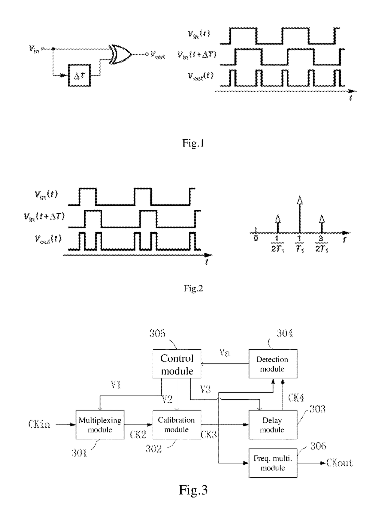
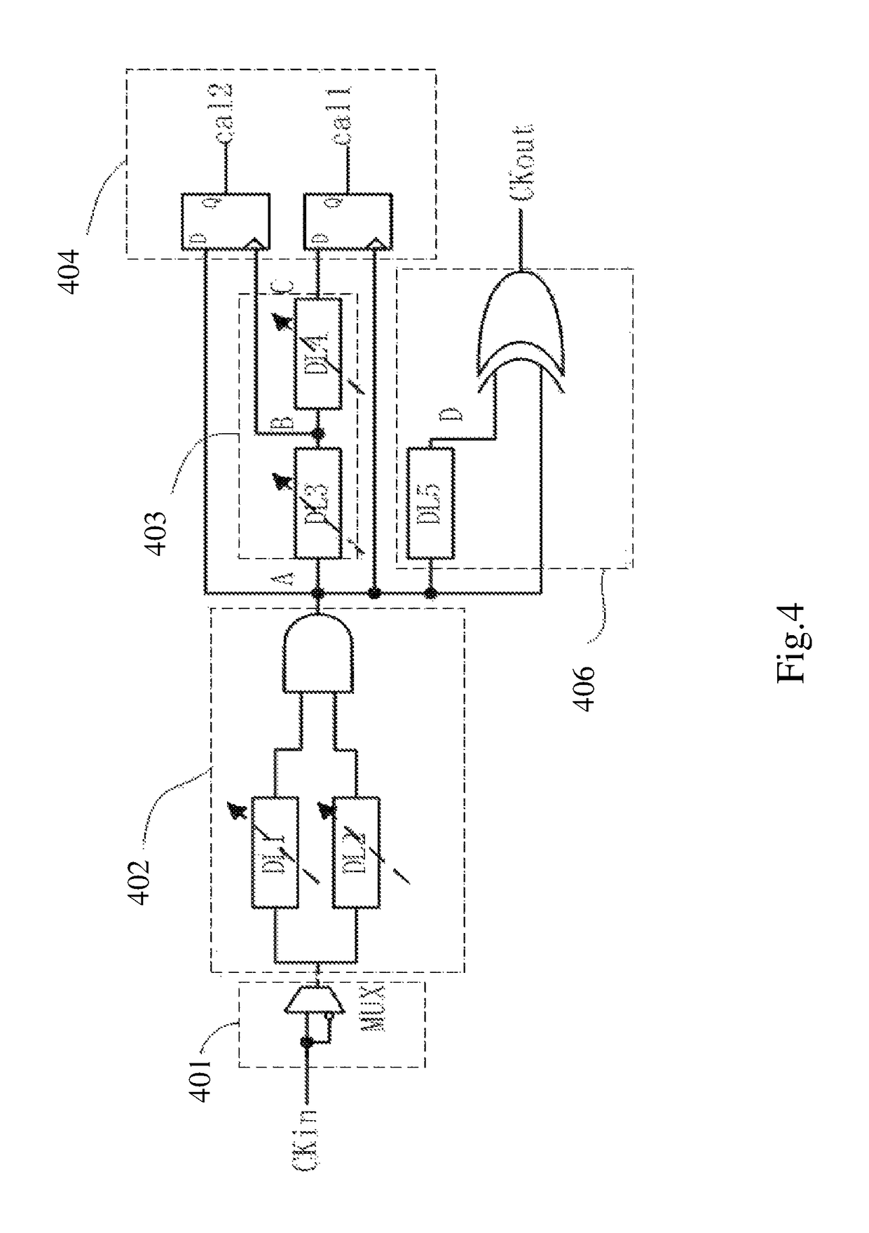
[0039]Referring to FIG. 3, the clock duty cycle calibration and frequency multiplier circuit according to the present invention includes a multiplexing module 301, a calibration module 302, a delay module 303, a detection module 304, a control module 305, and a frequency multiplication module 306.

[0040]The multiplexing module 301 inverts an input first clock signal CKin based on a first control signal V1, then outputs a second clock signal CK2 to the calibration module 302. In an implementation, the multiplexing m...


PUM


Abstract

A clock duty cycle calibration and frequency multiplier circuit used in a square wave frequency multiplier has a multiplexing module, which performs a phase-inversion operation on a clock signal according to a control signal; a calibration module which adjusts the duty cycle according to a control signal, and outputs a clock signal with a 50% duty cycle; a delay module, which performs a delay operation on the clock signal according to a control signal; a detection module, which compares the clock signal and outputs a feedback signal; a control module, which outputs a control signal according to the feedback signal; a frequency multiplication module, which performs a frequency multiplication operation on the clock signal. Therefore, high-precision clock signal frequency multiplication is implemented with relatively low circuit complexity and low cost.

Description

TECHNICAL FIELD[0001]The present invention relates to the field of integrated circuit technologies, and more particularly to a clock duty cycle calibration and frequency multiplier circuit used in a square wave frequency multiplier.BACKGROUND OF THE INVENTION[0002]In the field of radio communications and the field of clock signal generation, in order to achieve lower low in-band phase noise and high-frequency quantization noise, a clock signal frequency multiplication technology is required for reducing multiples of frequency multiplication of a phase-locked loop. The clock signal frequency multiplication technology may be implemented in a manner of an analog circuit and a digital circuit.[0003]FIG. 1 shows a method of implementing clock signal frequency multiplication through a digital circuit. An exclusive-OR operation is performed on an input clock signal Vin and a clock signal obtained after the Vin being delayed by ΔT, to obtain a frequency multiplication output clock signal Vo...

Claims


Application Information

Patent Timeline
Patent Type & Authority Patents(United States)
IPC IPC(8): H03K5/00H03K19/20H03L7/085H03K5/156
CPCH03K5/1565H03L7/085H03K5/00006H03K19/20H03K3/017
Inventor FU, ZHUOJIAN
Owner ALLWINNER TECH CO LTD
Why Eureka
Try Eureka