Copper foil provided with carrier, laminate, printed wiring board, electronic device, and method for fabricating printed wiring board

a technology of printed wiring and copper foil, which is applied in the direction of printed circuit manufacturing, printed element electric connection formation, metallic pattern materials, etc., can solve the problems of low mechanical strength of ultrathin copper foil, disconnection of circuits, and high cost, and achieve the effect of suppressing the disconnection of circuits and fine circuits

Active Publication Date: 2019-01-22
JX NIPPON MINING & METALS CORP
View PDF20 Cites 3 Cited by
  • Summary
  • Abstract
  • Description
  • Claims
  • Application Information

AI Technical Summary

Benefits of technology

[0055]According to the present invention, a copper foil provided with a carrier can be provided which enables to form an extremely fine circuit and to suppress the disconnection of a circuit well.

Problems solved by technology

Recently, while a copper foil having a thickness of 9 μm or less, or even a thickness of 5 μm or less has been required to cope with a fine pitch, such an ultrathin copper foil has a low mechanical strength, and is likely to tear or generate a wrinkle in fabricating a printed wiring board.
In addition, pinholes are likely to be generated in the surface of the ultrathin copper layer of a copper foil provided with a carrier due to the thinness.
The generation of such pinholes may cause the disconnection of a circuit.

Method used


Image

  • Copper foil provided with carrier, laminate, printed wiring board, electronic device, and method for fabricating printed wiring board
  • Copper foil provided with carrier, laminate, printed wiring board, electronic device, and method for fabricating printed wiring board
  • Copper foil provided with carrier, laminate, printed wiring board, electronic device, and method for fabricating printed wiring board

Examples


examples

[0350]Hereinafter, the present invention will be described in more detail using Examples of the present invention, but the present invention is never limited to these Examples in any way.

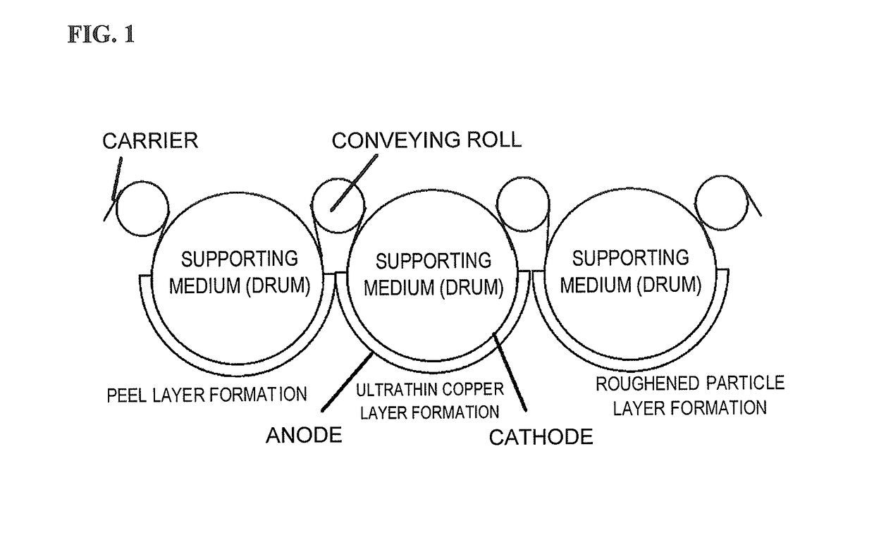
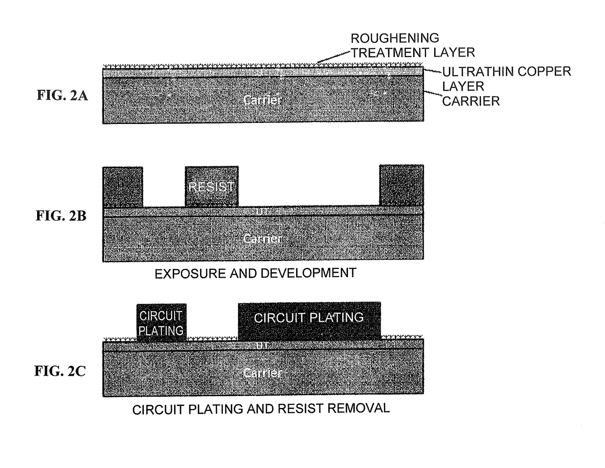
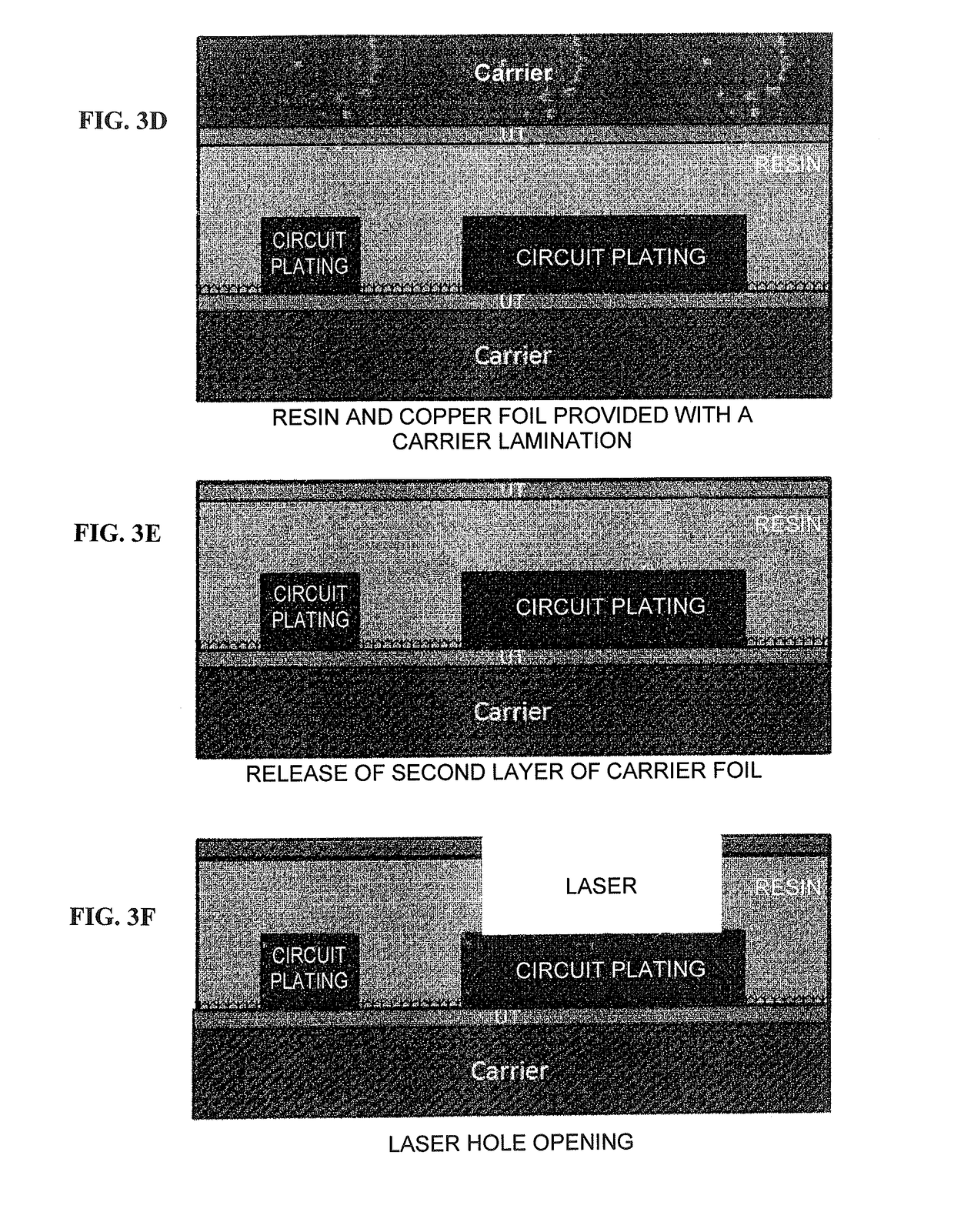
1. Fabrication of Copper Foil Provided with Carrier

[0351]A long copper foil or aluminum foil or polyimide film having a thickness listed in Tables 1 and 4 was prepared as a carrier. For “Electrolytic copper foil”, “Rolled copper foil” and “Aluminum foil” in Tables were used an electrolytic copper foil manufactured by JX Nippon Mining & Metals Corporation, a Tough Pitch Copper foil manufactured by JX Nippon Mining & Metals Corporation and a commercially available aluminum foil of alloy number 1N30 defined in JIS H4160 1994, respectively. For “Polyimide film” was used a polyimide film obtained by soaking a polyimide film (Apical NPI manufactured by Kaneka Corporation) in an aqueous solution containing 3 mol / L of hydrazine monohydrate and 3 mol / L of sodium hydroxide at 25° C. for 60 seconds to hydrophi...


PUM

PropertyMeasurementUnit
thicknessaaaaaaaaaa
thicknessaaaaaaaaaa
thicknessaaaaaaaaaa

Abstract

Provided is a copper foil provided with a carrier which enables to form an extremely fine circuit and to suppress the disconnection of a circuit well. A copper foil provided with a carrier having, in order, an intermediate layer and an ultrathin copper layer on one side or both sides of the carrier, wherein the ultrathin copper layer is an electrolytic copper layer; and the thickness of the ultrathin copper layer measured by using a gravimetric method is 1.5 μm or less and the number of pinholes in the ultrathin copper layer is 0 pinholes / m2 or more and 5 pinholes / m2 or less.

Description

TECHNICAL FIELD[0001]The present invention relates to a copper foil provided with a carrier, a laminate, a printed wiring board, an electronic device, and a method for fabricating a printed wiring board.[0002]In general, a printed wiring board is fabricated through steps in which an insulating substrate is adhered to a copper foil to make a copper-clad laminate and a conductive pattern is formed on the copper foil surface by etching. High-density implementation of mounted components and handling of signals at higher frequencies have been progressed along with the increase of the recent needs for smaller electronic devices with a higher performance, and printed wiring boards are needed to have a fine conductive pattern (fine pitch) and to deal with high frequencies.[0003]Recently, while a copper foil having a thickness of 9 μm or less, or even a thickness of 5 μm or less has been required to cope with a fine pitch, such an ultrathin copper foil has a low mechanical strength, and is l...

Claims


Application Information

Patent Timeline
Patent Type & Authority Patents(United States)
IPC IPC(8): H05K1/09H05K3/20H05K3/42H05K3/40H05K3/02
CPCH05K1/09H05K3/205H05K2203/0307H05K3/4007H05K3/421H05K3/025C25D7/0614H05K3/108
Inventor KOHIKI, MICHIYANAGAURA, TOMOTA
Owner JX NIPPON MINING & METALS CORP
Why Eureka
Try Eureka